
Electronics and Communication Engineering
GATE ECE BJT and MOSFET amplifiers PYQs
Build your understanding with focused practice from past exam papers.
How to practice BJT and MOSFET amplifiers
Attempt a question, record the concept and assumptions, then check the available answer. Rework mistakes after revising the relevant concepts. Topic tags can overlap; review the question context.
Questions 1–10 of 33. Imported answers require independent review unless marked reviewed.
Question 18
Open questionECMCQ1 markNeeds review
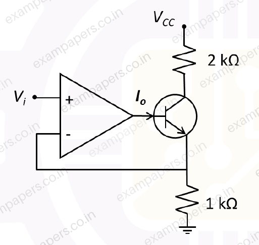
Consider the circuit shown in the Figure with
and
.Assume
and
for the BJT.Which of the following options is the correct value of the current
? 
Your answerChoose one option.
Log in to check the answer
You can attempt this question now. Sign in to view the answer key, explanations and discussion.Log in to check answerQuestion 29
Open questionECMSQ1 markNeeds review
Figure shows the output characteristics of two different Bipolar Junction Transistors (BJT), BJT 1 with magnitude of Early voltage
, and BJT 2 with magnitude of Early voltage
. Which of the following options is/are correct regarding the Early voltages? 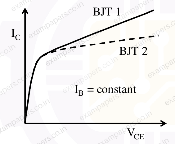
Your answerSelect all correct options. You can choose more than one.
Log in to check the answer
You can attempt this question now. Sign in to view the answer key, explanations and discussion.Log in to check answerQuestion 50
Open questionECMCQ2 marksNeeds review
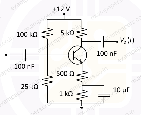
A small signal source,
is applied to a BJT circuit as shown in the Figure.Assume zero source resistance,
V,
, Early voltage = 100 V and Thermal voltage = 25 mV. Effect of internal parasitic capacitances of the BJT may be neglected.Which expression is the best approximation of the output voltage
? 
Your answerChoose one option.
Log in to check the answer
You can attempt this question now. Sign in to view the answer key, explanations and discussion.Log in to check answerQuestion 21
Open questionECMCQ1 markNeeds review
A simplified small-signal equivalent circuit of a BJT-based amplifier is given below. The small-signal voltage gain
(in V/V) is ________. 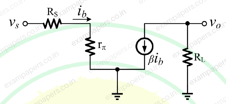
Your answerChoose one option.
Log in to check the answer
You can attempt this question now. Sign in to view the answer key, explanations and discussion.Log in to check answerQuestion 22
Open questionECMCQ1 markNeeds review
The ideal BJT in the circuit given below is biased in the active region with a
of 100. If
is 10
A, then
(in Volts, rounded off to two decimal places) is ______ . 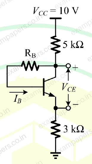
Your answerChoose one option.
Log in to check the answer
You can attempt this question now. Sign in to view the answer key, explanations and discussion.Log in to check answerQuestion 30
Open questionECMSQ1 markNeeds review
Which of the following statements is/are TRUE with respect to ideal MOSFET-based DC-coupled single-stage amplifiers having finite load resistors?
Your answerSelect all correct options. You can choose more than one.
Log in to check the answer
You can attempt this question now. Sign in to view the answer key, explanations and discussion.Log in to check answerQuestion 43
Open questionECMCQ2 marksNeeds review
The identical MOSFETs M₁ and M₂ in the circuit given below are ideal and biased in the saturation region. M₁ and M₂ have a transconductance
of 5 mS.The input signals (in Volts) are:
The output signal
(in Volts) is ________. 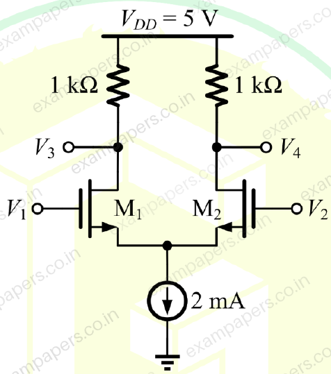
Your answerChoose one option.
Log in to check the answer
You can attempt this question now. Sign in to view the answer key, explanations and discussion.Log in to check answerQuestion 47
Open questionECMCQ2 marksNeeds review
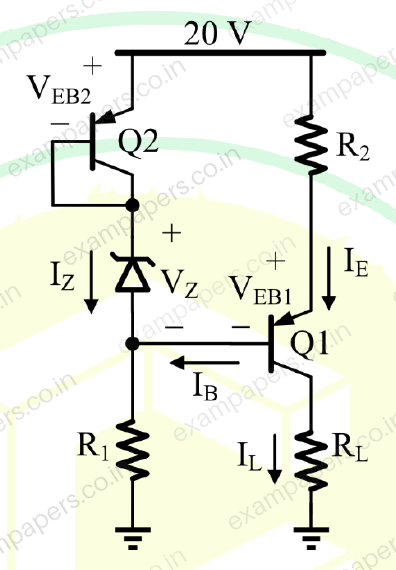
In the circuit shown, the identical transistors Q1 and Q2 are biased in the active region with β = 120. The Zener diode is in the breakdown region with VZ = 5 V and IZ = 25 mA.
If IL = 12 mA and VEB1 = VEB2 = 0.7 V, then the values of R1 and R2 (in kΩ, rounded off to one decimal place) are ______, respectively.
Your answerChoose one option.
Log in to check the answer
You can attempt this question now. Sign in to view the answer key, explanations and discussion.Log in to check answerQuestion 17
Open questionECMCQ1 markNeeds review
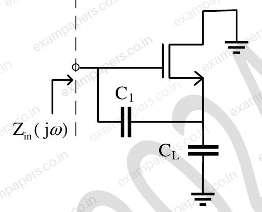
In the circuit below, assume that the long channel NMOS transistor is biased in saturation. The small signal trans-conductance for the transistor is
. Neglect body effect, channel length modulation and intrinsic device capacitances. The small signal input impedance
is ______.
Your answerChoose one option.
Log in to check the answer
You can attempt this question now. Sign in to view the answer key, explanations and discussion.Log in to check answerQuestion 18
Open questionECMCQ1 markNeeds review
For the closed loop amplifier circuit shown below, the magnitude of open loop low frequency small signal voltage gain is 40.
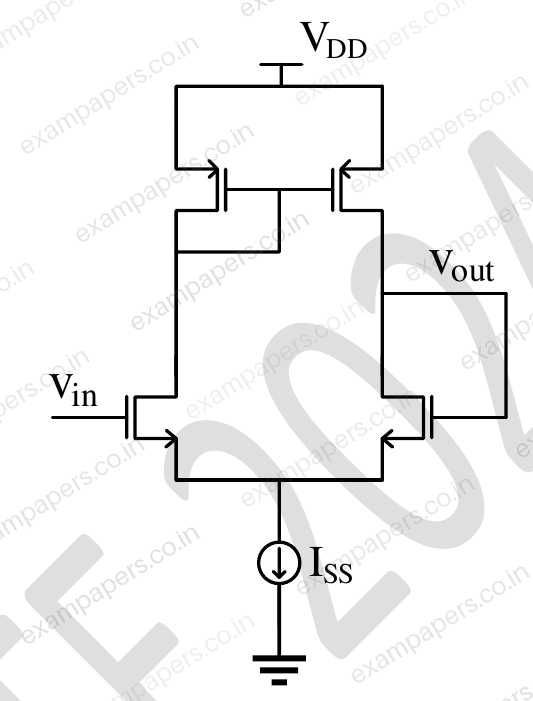
All the transistors are biased in saturation. The current source
is ideal. Neglect body effect, channel length modulation and intrinsic device capacitances. The closed loop low frequency small signal voltage gain
(rounded off to three decimal places) is ____.Your answerChoose one option.
Log in to check the answer
You can attempt this question now. Sign in to view the answer key, explanations and discussion.Log in to check answer