
Electronics and Communication Engineering
GATE ECE Combinational circuits PYQs
Build your understanding with focused practice from past exam papers.
How to practice Combinational circuits
Attempt a question, record the concept and assumptions, then check the available answer. Rework mistakes after revising the relevant concepts. Topic tags can overlap; review the question context.
Questions 1–10 of 19. Imported answers require independent review unless marked reviewed.
Question 19
Open questionECMCQ1 markNeeds review
For the Boolean function
the essential prime implicants are __________.Your answerChoose one option.
Log in to check the answer
You can attempt this question now. Sign in to view the answer key, explanations and discussion.Log in to check answerQuestion 40
Open questionECMCQ2 marksNeeds review
A 4-bit priority encoder has inputs
, and
in descending order of priority. The two-bit output
is generated as 00, 01, 10, and 11 corresponding to inputs
, and
, respectively. The Boolean expression of the output bit
is ______.Your answerChoose one option.
Log in to check the answer
You can attempt this question now. Sign in to view the answer key, explanations and discussion.Log in to check answerQuestion 41
Open questionECMCQ2 marksNeeds review
The propagation delay of the
MUX shown in the circuit is 10 ns. Consider the propagation delay of the inverter as 0 ns. 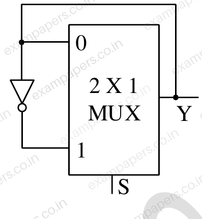
If
is set to 1 then the output
is ______.Your answerChoose one option.
Log in to check the answer
You can attempt this question now. Sign in to view the answer key, explanations and discussion.Log in to check answerQuestion 19
Open questionECMCQ1 markNeeds review
Consider the 2-bit multiplexer (MUX) shown in the figure. For OUTPUT to be the XOR of C and D, the values for
,
,
, and
are ____________. 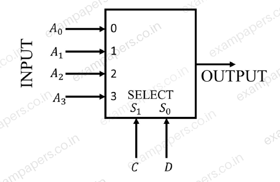
Your answerChoose one option.
Log in to check the answer
You can attempt this question now. Sign in to view the answer key, explanations and discussion.Log in to check answerQuestion 27
Open questionECMSQ1 markNeeds review
Select the Boolean function(s) equivalent to
, where
,
and
are Boolean variables, and + denotes logical OR operation.Your answerSelect all correct options. You can choose more than one.
Log in to check the answer
You can attempt this question now. Sign in to view the answer key, explanations and discussion.Log in to check answerQuestion 28
Open questionECMSQ1 markNeeds review
Select the correct statement(s) regarding CMOS implementation of NOT gates.
Your answerSelect all correct options. You can choose more than one.
Log in to check the answer
You can attempt this question now. Sign in to view the answer key, explanations and discussion.Log in to check answerQuestion 49
Open questionECMSQ2 marksNeeds review
Consider a Boolean gate (D) where the output
is related to the inputs
and
as
, where + denotes logical OR operation. The Boolean inputs ‘0’ and ‘1’ are also available separately. Using instances of only D gates and inputs ‘0’ and ‘1’, ______ (select the correct option(s)).Your answerSelect all correct options. You can choose more than one.
Log in to check the answer
You can attempt this question now. Sign in to view the answer key, explanations and discussion.Log in to check answerQuestion 13
Open questionECMCQ1 markNeeds review
A standard CMOS inverter is designed with equal rise and fall times (
). If the width of the PMOS transistor in the inverter is increased, what would be the effect on the LOW noise margin (
) and the HIGH noise margin (
)?Your answerChoose one option.
Log in to check the answer
You can attempt this question now. Sign in to view the answer key, explanations and discussion.Log in to check answerQuestion 14
Open questionECMCQ1 markNeeds review
In the circuit shown, what are the values of F for EN = 0 and EN = 1, respectively?
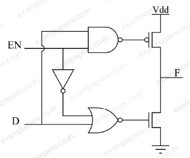
Your answerChoose one option.
Log in to check the answer
You can attempt this question now. Sign in to view the answer key, explanations and discussion.Log in to check answerQuestion 15
Open questionECMCQ1 markNeeds review
In the circuit shown, A and B are the inputs and F is the output. What is the functionality of the circuit?
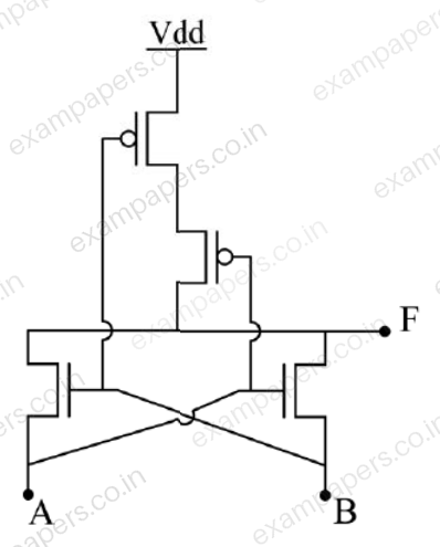
Your answerChoose one option.
Log in to check the answer
You can attempt this question now. Sign in to view the answer key, explanations and discussion.Log in to check answer