
Electronics and Communication Engineering
GATE ECE format:nat PYQs
Build your understanding with focused practice from past exam papers.
Questions 41–50 of 239. Imported answers require independent review unless marked reviewed.
Question 63
Open questionECNAT2 marksNeeds review
A non-degenerate n-type semiconductor has 5% neutral dopant atoms. Its Fermi level is located at 0.25 eV below the conduction band (
) and the donor energy level (
) has a degeneracy of 2. Assuming the thermal voltage to be 20 mV, the difference between
and
(in eV, rounded off to two decimal places) is __________.Log in to check the answer
You can attempt this question now. Sign in to view the answer key, explanations and discussion.Log in to check answerQuestion 64
Open questionECNAT2 marksNeeds review
An NMOS transistor operating in the linear region has
of 5
A at
of 0.1 V. Keeping
constant, the
is increased to 1.5 V.Given that
, the transconductance at the new operating point (in
A/V, rounded off to two decimal places) is ______.Log in to check the answer
You can attempt this question now. Sign in to view the answer key, explanations and discussion.Log in to check answerQuestion 65
Open questionECNAT2 marksNeeds review
The photocurrent of a PN junction diode solar cell is 1 mA. The voltage corresponding to its maximum power point is 0.3 V. If the thermal voltage is 30 mV, the reverse saturation current of the diode (in nA, rounded off to two decimal places) is ______.
Log in to check the answer
You can attempt this question now. Sign in to view the answer key, explanations and discussion.Log in to check answerQuestion 31
Open questionECNAT1 markNeeds review
The signal-to-noise ratio (SNR) of an ADC with a full-scale sinusoidal input is given to be 61.96 dB. The resolution of the ADC is ______ bits (rounded off to the nearest integer).
Log in to check the answer
You can attempt this question now. Sign in to view the answer key, explanations and discussion.Log in to check answerQuestion 32
Open questionECNAT1 markNeeds review
In the circuit shown below, the current
flowing through 200
resistor is ______ mA (rounded off to two decimal places). 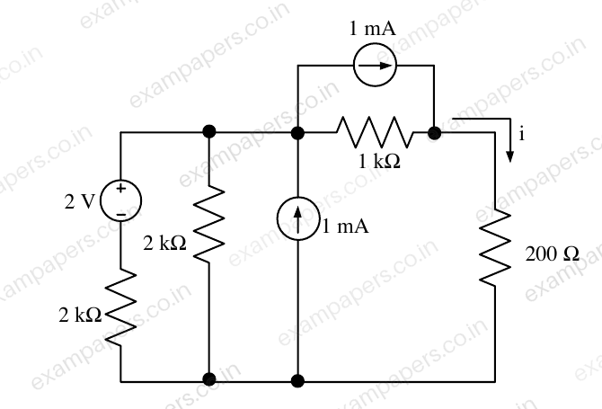
Log in to check the answer
You can attempt this question now. Sign in to view the answer key, explanations and discussion.Log in to check answerQuestion 33
Open questionECNAT1 markNeeds review
For the two port network shown below, the [Y]-parameters is given as
The value of load impedance
, in
, for maximum power transfer will be ______ (rounded off to the nearest integer). 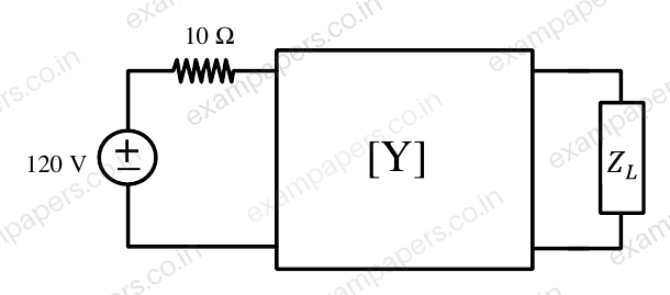
Log in to check the answer
You can attempt this question now. Sign in to view the answer key, explanations and discussion.Log in to check answerQuestion 34
Open questionECNAT1 markNeeds review
For the circuit shown below, the propagation delay of each NAND gate is 1 ns. The critical path delay, in ns, is ______ (rounded off to the nearest integer).
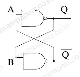
Log in to check the answer
You can attempt this question now. Sign in to view the answer key, explanations and discussion.Log in to check answerQuestion 35
Open questionECNAT1 markNeeds review
In the circuit shown below, switch S was closed for a long time. If the switch is opened at
, the maximum magnitude of the voltage
, in volts, is ______ (rounded off to the nearest integer). 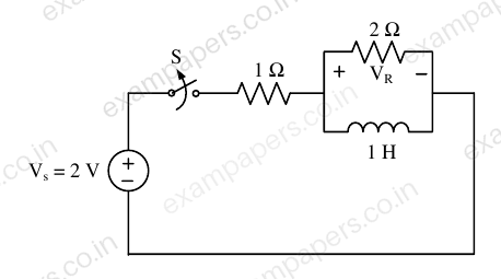
Log in to check the answer
You can attempt this question now. Sign in to view the answer key, explanations and discussion.Log in to check answerQuestion 55
Open questionECNAT2 marksNeeds review
The value of the integral
over the region R, given in the figure
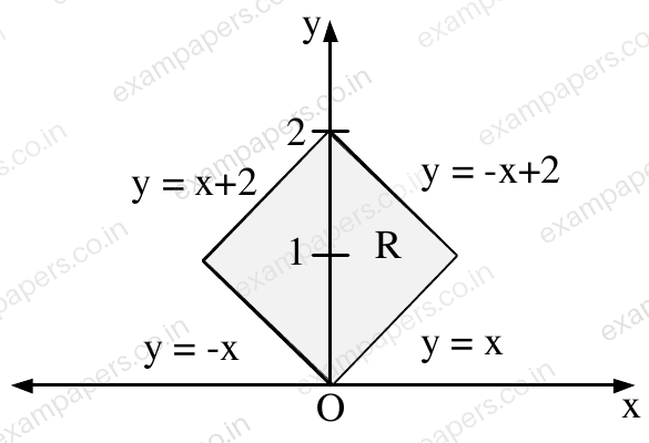
, is ______ (rounded off to the nearest integer).
Log in to check the answer
You can attempt this question now. Sign in to view the answer key, explanations and discussion.Log in to check answerQuestion 56
Open questionECNAT2 marksNeeds review
In an extrinsic semiconductor, the hole concentration is given to be
where
is the intrinsic carrier concentration of
. The ratio of electron to hole mobility for equal hole and electron drift current is given as ______ (rounded off to two decimal places).Log in to check the answer
You can attempt this question now. Sign in to view the answer key, explanations and discussion.Log in to check answer