
Electronics and Communication Engineering
GATE ECE kind:question PYQs
Build your understanding with focused practice from past exam papers.
Questions 471–480 of 715. Imported answers require independent review unless marked reviewed.
Question 6
Open questionECMCQ1 markNeeds review
For an LTI system, the Bode plot for its gain is as illustrated in the figure shown. The number of system poles
and the number of system zeros
in the frequency range
is 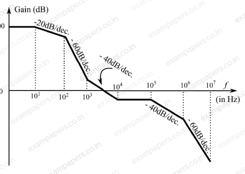
Your answerChoose one option.
Log in to check the answer
You can attempt this question now. Sign in to view the answer key, explanations and discussion.Log in to check answerQuestion 7
Open questionECMCQ1 markNeeds review
A linear Hamming code is used to map 4-bit messages to 7-bit codewords. The encoder mapping is linear. If the message 0001 is mapped to the codeword 0000111, and the message 0011 is mapped to the codeword 110010, then the message 0010 is mapped to
Your answerChoose one option.
Log in to check the answer
You can attempt this question now. Sign in to view the answer key, explanations and discussion.Log in to check answerQuestion 8
Open questionECMCQ1 markNeeds review
Which one of the following options describes correctly the equilibrium band diagram at
of a Silicon
configuration shown in the figure? 
Your answerChoose one option.
Log in to check the answer
You can attempt this question now. Sign in to view the answer key, explanations and discussion.Log in to check answerQuestion 9
Open questionECMCQ1 markNeeds review
The correct circuit representation of the structure shown in the figure is
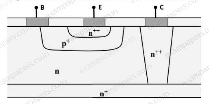
Your answerChoose one option.
Log in to check the answer
You can attempt this question now. Sign in to view the answer key, explanations and discussion.Log in to check answerQuestion 10
Open questionECMCQ1 markNeeds review
The figure shows the high-frequency C-V curve of a MOS capacitor (at T = 300 K) with
and no oxide charges. The flat-band, inversion, and accumulation conditions are represented, respectively, by the points
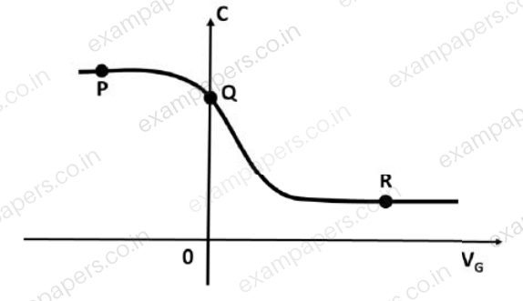
Your answerChoose one option.
Log in to check the answer
You can attempt this question now. Sign in to view the answer key, explanations and discussion.Log in to check answerQuestion 11
Open questionECMCQ1 markNeeds review
What is the electric flux (
) through a quarter-cylinder of height
(as shown in the figure) due to an infinitely long line charge along the axis of the cylinder with a charge density of
?
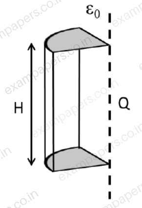
Your answerChoose one option.
Log in to check the answer
You can attempt this question now. Sign in to view the answer key, explanations and discussion.Log in to check answerQuestion 12
Open questionECMCQ1 markNeeds review
In the table shown, List I and List II, respectively, contain terms appearing on the left-hand side and the right-hand side of Maxwell’s equations (in their standard form). Match the left-hand side with the corresponding right-hand side.
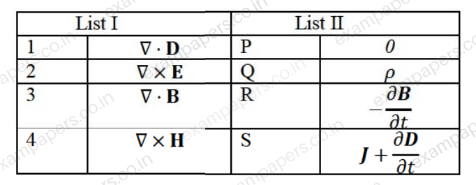
Your answerChoose one option.
Log in to check the answer
You can attempt this question now. Sign in to view the answer key, explanations and discussion.Log in to check answerQuestion 13
Open questionECMCQ1 markNeeds review
A standard CMOS inverter is designed with equal rise and fall times (
). If the width of the PMOS transistor in the inverter is increased, what would be the effect on the LOW noise margin (
) and the HIGH noise margin (
)?Your answerChoose one option.
Log in to check the answer
You can attempt this question now. Sign in to view the answer key, explanations and discussion.Log in to check answerQuestion 14
Open questionECMCQ1 markNeeds review
In the circuit shown, what are the values of F for EN = 0 and EN = 1, respectively?
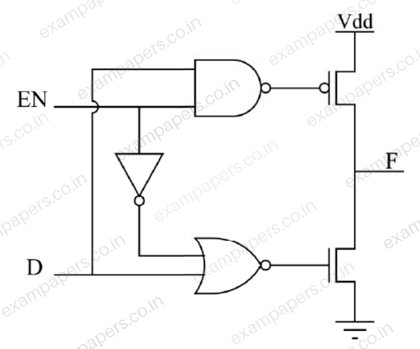
Your answerChoose one option.
Log in to check the answer
You can attempt this question now. Sign in to view the answer key, explanations and discussion.Log in to check answerQuestion 15
Open questionECMCQ1 markNeeds review
In the circuit shown, A and B are the inputs and F is the output. What is the functionality of the circuit?
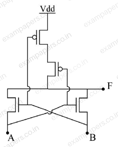
Your answerChoose one option.
Log in to check the answer
You can attempt this question now. Sign in to view the answer key, explanations and discussion.Log in to check answer