
Electronics and Communication Engineering
GATE ECE kind:question PYQs
Build your understanding with focused practice from past exam papers.
Questions 611–620 of 715. Imported answers require independent review unless marked reviewed.
Question 13
Open questionECMCQ1 markNeeds review
In the figure, D1 is a real silicon
junction diode with a drop of 0.7 V under forward bias condition and D2 is a Zener diode with breakdown voltage of
V. The input
is a periodic square wave of period T, whose one period is shown in the figure. 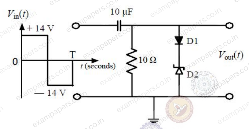
Assuming
, where
is the time constant of the circuit, the maximum and minimum values of the output waveform are respectivelyYour answerChoose one option.
Log in to check the answer
You can attempt this question now. Sign in to view the answer key, explanations and discussion.Log in to check answerQuestion 14
Open questionECMCQ1 markNeeds review
The Miller effect in the context of a Common Emitter amplifier explains
Your answerChoose one option.
Log in to check the answer
You can attempt this question now. Sign in to view the answer key, explanations and discussion.Log in to check answerQuestion 14
Open questionECNAT1 markNeeds review
Consider the circuit shown in the figure. Assume base-to-emitter voltage
and common-base current gain
of the transistor is unity. 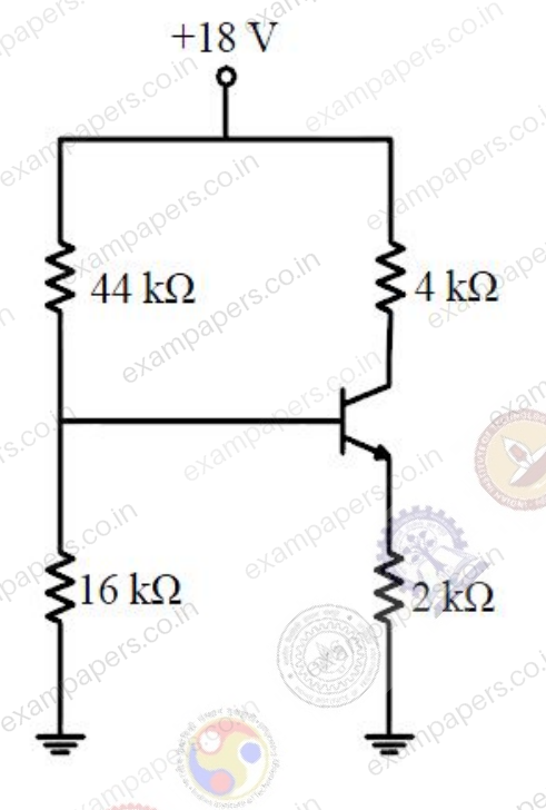
The value of the collector-to-emitter voltage
(in volt) is _____.Log in to check the answer
You can attempt this question now. Sign in to view the answer key, explanations and discussion.Log in to check answerQuestion 15
Open questionECMCQ1 markNeeds review
In the latch circuit shown, the NAND gates have non-zero, but unequal propagation delays. The present input condition is: P = Q = ‘0’. If the input condition is changed simultaneously to P = Q = ‘1’, the outputs X and Y are
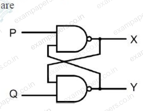
Your answerChoose one option.
Log in to check the answer
You can attempt this question now. Sign in to view the answer key, explanations and discussion.Log in to check answerQuestion 15
Open questionECMCQ1 markNeeds review
For the circuit shown in the figure,
and
are the inputs and
is the output. 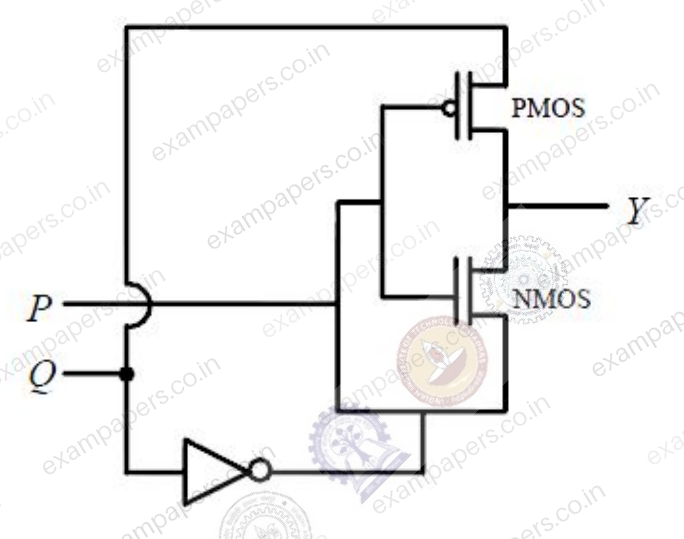
The logic implemented by the circuit is
Your answerChoose one option.
Log in to check the answer
You can attempt this question now. Sign in to view the answer key, explanations and discussion.Log in to check answerQuestion 16
Open questionECMCQ1 markNeeds review
The clock frequency of an 8085 microprocessor is 5 MHz. If the time required to execute an instruction is 1.4 μs, then the number of T-states needed for executing the instruction is
Your answerChoose one option.
Log in to check the answer
You can attempt this question now. Sign in to view the answer key, explanations and discussion.Log in to check answerQuestion 16
Open questionECMCQ1 markNeeds review
Consider the circuit shown in the figure.
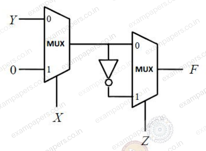
The Boolean expression
implemented by the circuit isYour answerChoose one option.
Log in to check the answer
You can attempt this question now. Sign in to view the answer key, explanations and discussion.Log in to check answerQuestion 17
Open questionECNAT1 markNeeds review
Consider the D-Latch shown in the figure, which is transparent when its clock input CK is high and has zero propagation delay. In the figure, the clock signal CLK1 has a 50% duty cycle and CLK2 is a one-fifth period delayed version of CLK1. The duty cycle at the output of the latch in percentage is
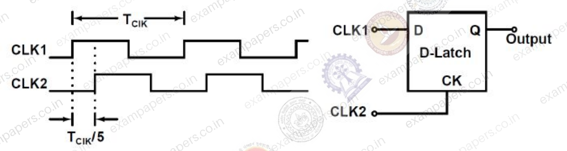
.
Log in to check the answer
You can attempt this question now. Sign in to view the answer key, explanations and discussion.Log in to check answerQuestion 17
Open questionECMCQ1 markNeeds review
In a DRAM,
Your answerChoose one option.
Log in to check the answer
You can attempt this question now. Sign in to view the answer key, explanations and discussion.Log in to check answerQuestion 18
Open questionECNAT1 markNeeds review
The open loop transfer function
where
is an integer, is connected in unity feedback configuration as shown in the figure. 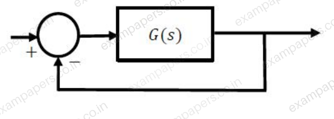
Given that the steady state error is zero for unit step input and is 6 for unit ramp input, the value of the parameter
is __________.Log in to check the answer
You can attempt this question now. Sign in to view the answer key, explanations and discussion.Log in to check answer