
Electronics and Communication Engineering
GATE ECE topic:bjt-mosfet-amplifiers PYQs
Build your understanding with focused practice from past exam papers.
Questions 11–20 of 33. Imported answers require independent review unless marked reviewed.
Question 51
Open questionECMCQ2 marksNeeds review
In the circuit shown below, the transistors
and
are biased in saturation. Their small signal transconductances are
and
respectively. Neglect body effect, channel length modulation and intrinsic device capacitances.
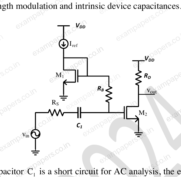
Assuming that capacitor
is a short circuit for AC analysis, the exact magnitude of small signal voltage gain
is ______.Your answerChoose one option.
Log in to check the answer
You can attempt this question now. Sign in to view the answer key, explanations and discussion.Log in to check answerQuestion 21
Open questionECMCQ1 markNeeds review
In the circuit shown below,
and
are bias voltages. Based on input and output impedances, the circuit behaves as a 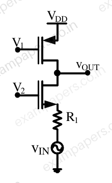
Your answerChoose one option.
Log in to check the answer
You can attempt this question now. Sign in to view the answer key, explanations and discussion.Log in to check answerQuestion 22
Open questionECMCQ1 markNeeds review
A cascade of common-source amplifiers in a unity gain feedback configuration oscillates when
Your answerChoose one option.
Log in to check the answer
You can attempt this question now. Sign in to view the answer key, explanations and discussion.Log in to check answerQuestion 64
Open questionECNAT2 marksNeeds review
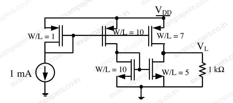
In the circuit below, the voltage
is __________ V (rounded off to two decimal places).
Log in to check the answer
You can attempt this question now. Sign in to view the answer key, explanations and discussion.Log in to check answerQuestion 59
Open questionECNAT2 marksNeeds review
Consider the circuit shown with an ideal long channel
MOSFET (enhancement-mode, substrate is connected to the source). The transistor is appropriately biased in the saturation region with
and
such that it acts as a linear amplifier.
is the small-signal ac input voltage.
and
represent the small-signal voltages at the nodes A and B, respectively. The value of
is ________ (rounded off to one decimal place). 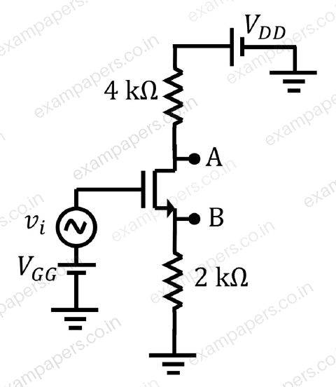
Log in to check the answer
You can attempt this question now. Sign in to view the answer key, explanations and discussion.Log in to check answerQuestion 8
Open questionECMCQ1 markNeeds review
In the circuit shown in the figure, the transistors
and
are operating in saturation. The channel length modulation coefficients of both the transistors are non-zero. The transconductance of the MOSFETs
and
are
and
, respectively, and the internal resistance of the MOSFETs
and
are
and
, respectively. 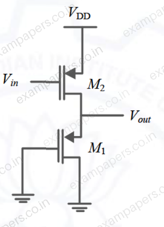
Ignoring the body effect, the ac small signal voltage gain (
) of the circuit isYour answerChoose one option.
Log in to check the answer
You can attempt this question now. Sign in to view the answer key, explanations and discussion.Log in to check answerQuestion 35
Open questionECMCQ2 marksNeeds review
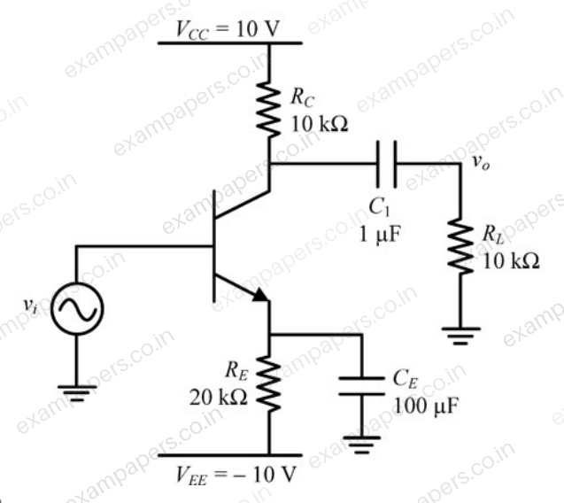
For the BJT in the amplifier shown below,
V,
mV. Assume that BJT output resistance (
) is very high and the base current is negligible. The capacitors are also assumed to be short circuited at signal frequencies. The input
is direct coupled. The low frequency voltage gain
of the amplifier is
Your answerChoose one option.
Log in to check the answer
You can attempt this question now. Sign in to view the answer key, explanations and discussion.Log in to check answerQuestion 37
Open questionECMCQ2 marksNeeds review
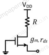
Using the incremental low frequency small-signal model of the MOS device, the Norton equivalent resistance of the following circuit is
Your answerChoose one option.
Log in to check the answer
You can attempt this question now. Sign in to view the answer key, explanations and discussion.Log in to check answerQuestion 44
Open questionECNAT2 marksNeeds review
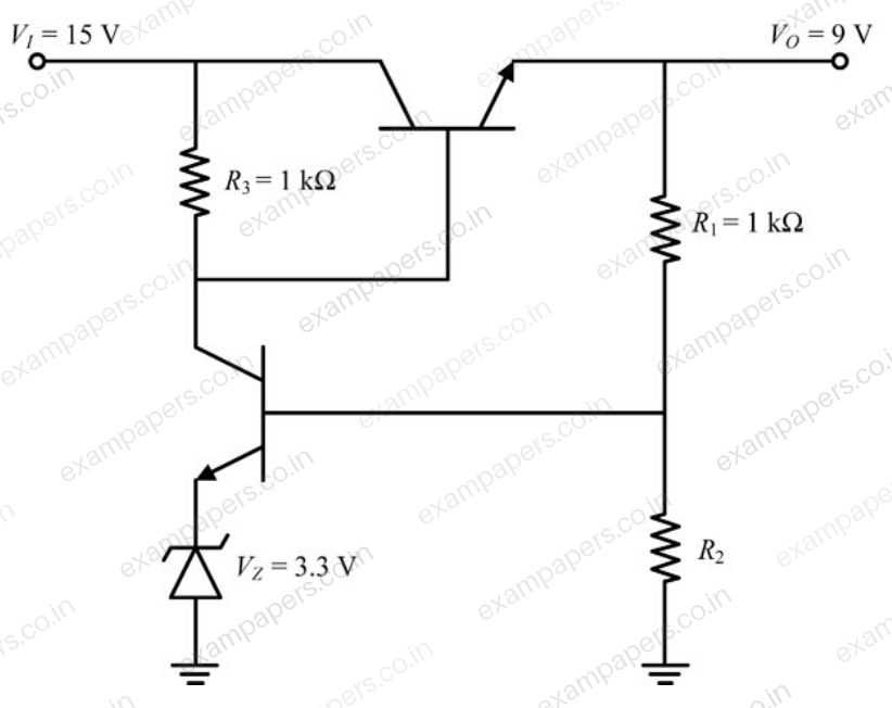
In the voltage regulator shown below, V_i is the unregulated input at 15 V. Assume V_BE = 0.7 V and the base current is negligible for both the BJTs. If the regulated output V_O is 9 V, the value of R₂ is ______ Ω.
Log in to check the answer
You can attempt this question now. Sign in to view the answer key, explanations and discussion.Log in to check answerQuestion 40
Open questionECMCQ2 marksNeeds review
In the circuits shown, the threshold voltage of each nMOS transistor is 0.6 V. Ignoring the effect of channel length modulation and body bias, the values of Vout1 and Vout2, respectively, in volts, are
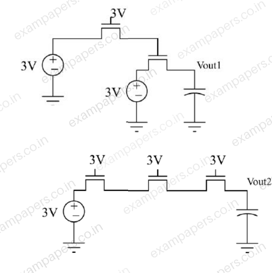
Your answerChoose one option.
Log in to check the answer
You can attempt this question now. Sign in to view the answer key, explanations and discussion.Log in to check answer