
Electronics and Communication Engineering
GATE ECE topic:electronics PYQs
Build your understanding with focused practice from past exam papers.
Questions 311–320 of 715. Imported answers require independent review unless marked reviewed.
Question 51
Open questionECMSQ2 marksNeeds review
Consider an FM broadcast that employs the pre-emphasis filter with frequency response
where
rad/sec. For the network shown in the figure to act as a corresponding de-emphasis filter, the appropriate pair(s) of
values is/are ______. 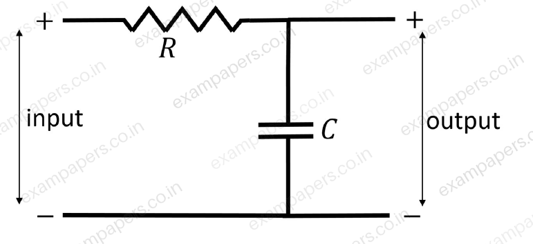
Your answerSelect all correct options. You can choose more than one.
Log in to check the answer
You can attempt this question now. Sign in to view the answer key, explanations and discussion.Log in to check answerQuestion 52
Open questionECMSQ2 marksNeeds review
A waveguide consists of two infinite parallel plates (perfect conductors) at a separation of
cm, with air as the dielectric. Assume the speed of light in air to be
m/s. The frequency/frequencies of TM wave which can propagate in this waveguide is/areYour answerSelect all correct options. You can choose more than one.
Log in to check the answer
You can attempt this question now. Sign in to view the answer key, explanations and discussion.Log in to check answerQuestion 53
Open questionECNAT2 marksNeeds review
The value of the integral
where
is the shaded triangular region shown in the diagram, is _____ (rounded off to the nearest integer). 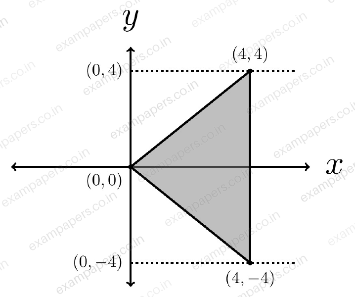
Log in to check the answer
You can attempt this question now. Sign in to view the answer key, explanations and discussion.Log in to check answerQuestion 54
Open questionECNAT2 marksNeeds review
A linear 2-port network is shown in Fig. (a). An ideal DC voltage source of 10 V is connected across Port 1. A variable resistance
is connected across Port 2. As
is varied, the measured voltage and current at Port 2 is shown in Fig. (b) as a
versus
plot. Note that for
V,
mA, and for
V,
mA.When the variable resistance
at Port 2 is replaced by the load shown in Fig. (c), the current
is ______ mA (rounded off to one decimal place). 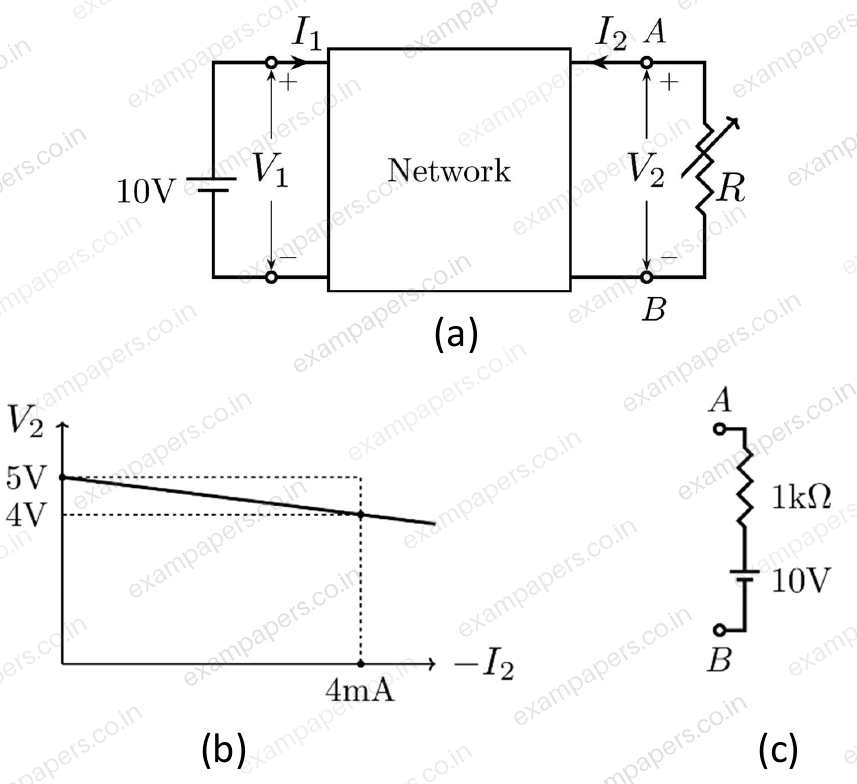
Log in to check the answer
You can attempt this question now. Sign in to view the answer key, explanations and discussion.Log in to check answerQuestion 55
Open questionECNAT2 marksNeeds review
For a vector
, the 8-point discrete Fourier transform (DFT) is denoted by
, where
Here,
. If
and
, then the value of
is ________ (rounded off to one decimal place).Log in to check the answer
You can attempt this question now. Sign in to view the answer key, explanations and discussion.Log in to check answerQuestion 56
Open questionECNAT2 marksNeeds review
A
-type semiconductor with zero electric field is under illumination (low level injection) in steady state condition. Excess minority carrier density is zero at
, where
cm is the diffusion length for electrons. Assume electronic charge,
C. The profiles of photo-generation rate of carriers and the recombination rate of excess minority carriers (
) are shown. Under these conditions, the magnitude of the current density due to the photo-generated electrons at
is ________ mA/cm
(rounded off to two decimal places). 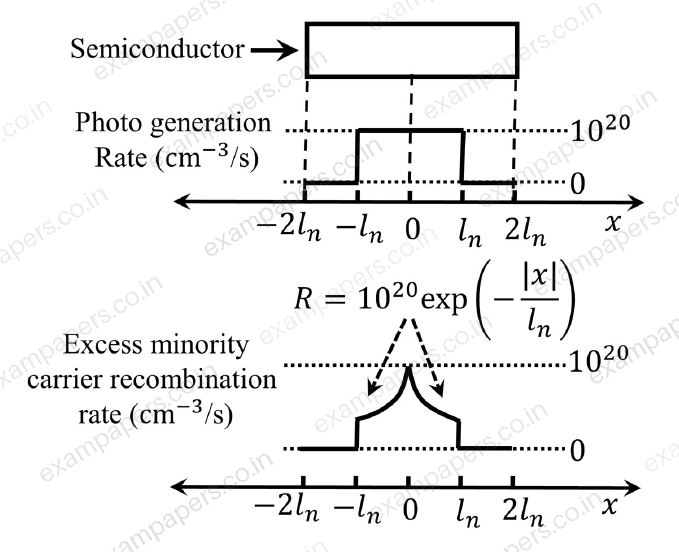
Log in to check the answer
You can attempt this question now. Sign in to view the answer key, explanations and discussion.Log in to check answerQuestion 57
Open questionECNAT2 marksNeeds review
A circuit and the characteristics of the diode (D) in it are shown. The ratio of the minimum to the maximum small signal voltage gain
is ________ (rounded off to two decimal places). 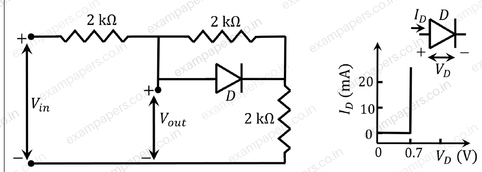
Log in to check the answer
You can attempt this question now. Sign in to view the answer key, explanations and discussion.Log in to check answerQuestion 58
Open questionECNAT2 marksNeeds review
Consider the circuit shown with an ideal OPAMP. The output voltage
is ________ V (rounded off to two decimal places). 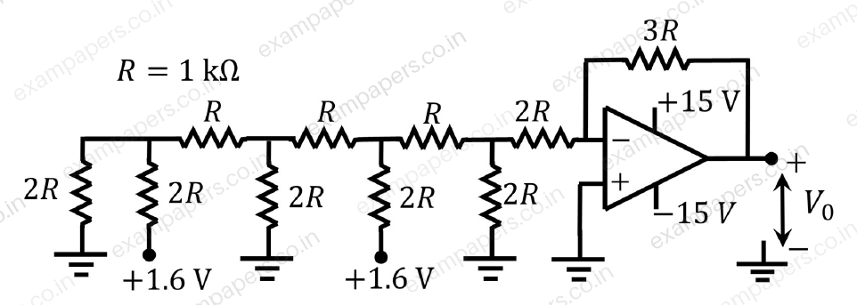
Log in to check the answer
You can attempt this question now. Sign in to view the answer key, explanations and discussion.Log in to check answerQuestion 59
Open questionECNAT2 marksNeeds review
Consider the circuit shown with an ideal long channel
MOSFET (enhancement-mode, substrate is connected to the source). The transistor is appropriately biased in the saturation region with
and
such that it acts as a linear amplifier.
is the small-signal ac input voltage.
and
represent the small-signal voltages at the nodes A and B, respectively. The value of
is ________ (rounded off to one decimal place). 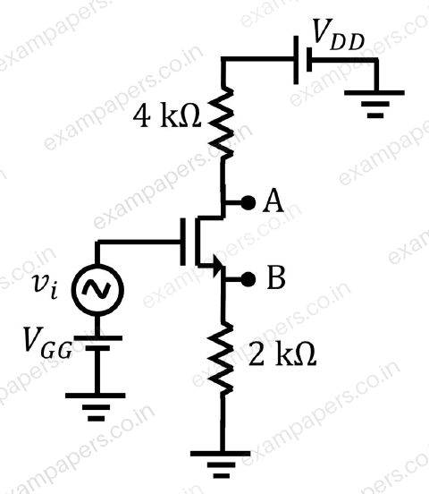
Log in to check the answer
You can attempt this question now. Sign in to view the answer key, explanations and discussion.Log in to check answerQuestion 60
Open questionECNAT2 marksNeeds review
The block diagram of a closed-loop control system is shown in the figure.
,
, and
are the Laplace transforms of the time-domain signals
,
, and
, respectively. Let the error signal be defined as
. Assuming the reference input
for all
, the steady-state error
, due to a unit step disturbance
, is ________ (rounded off to two decimal places). 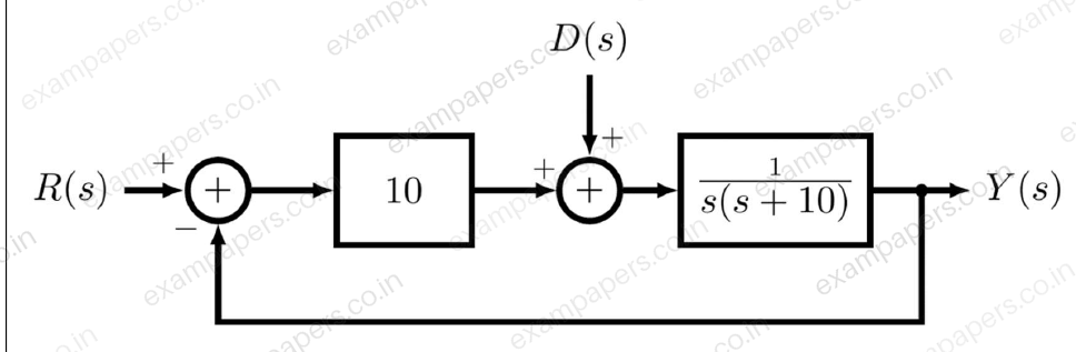
Log in to check the answer
You can attempt this question now. Sign in to view the answer key, explanations and discussion.Log in to check answer