
Electrical Engineering
GATE EE Analog and Digital Electronics PYQs
Build your understanding with focused practice from past exam papers.
Questions 51–57 of 57. Imported answers require independent review unless marked reviewed.
Question 35
Open questionEEMCQ2 marksNeeds review
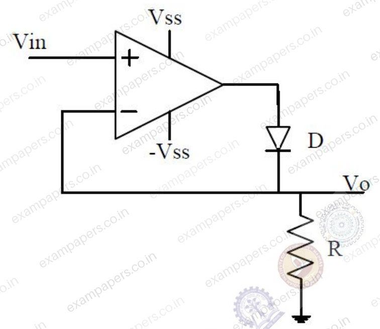
The approximate transfer characteristic for the circuit shown below with an ideal operational amplifier and diode will be
Your answerChoose one option.
Log in to check the answer
You can attempt this question now. Sign in to view the answer key, explanations and discussion.Log in to check answerQuestion 36
Open questionEEMCQ2 marksNeeds review
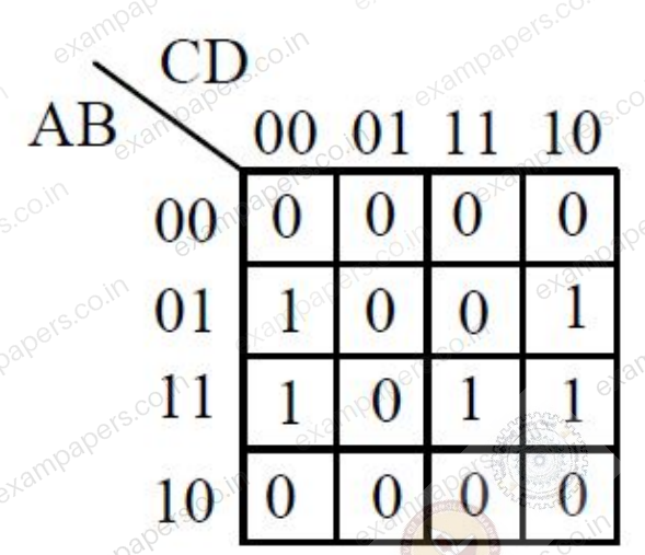
The output expression for the Karnaugh map shown below is
Your answerChoose one option.
Log in to check the answer
You can attempt this question now. Sign in to view the answer key, explanations and discussion.Log in to check answerQuestion 37
Open questionEEMCQ2 marksNeeds review
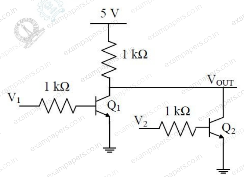
The logical gate implemented using the circuit shown below where, V₁ and V₂ are inputs (with 0 V as digital 0 and 5 V as digital 1) and Vₒᵤₜ is the output, is
Your answerChoose one option.
Log in to check the answer
You can attempt this question now. Sign in to view the answer key, explanations and discussion.Log in to check answerQuestion 37
Open questionEE-2MCQ2 marksNeeds review
For the circuit shown in the figure below, it is given that
. The transistor has
and
when the B-E junction is forward biased. 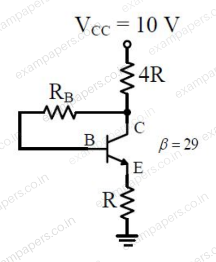
For this circuit, the value of
isYour answerChoose one option.
Log in to check the answer
You can attempt this question now. Sign in to view the answer key, explanations and discussion.Log in to check answerQuestion 38
Open questionEE-2MCQ2 marksNeeds review
For the circuit shown below, assume that the OPAMP is ideal.
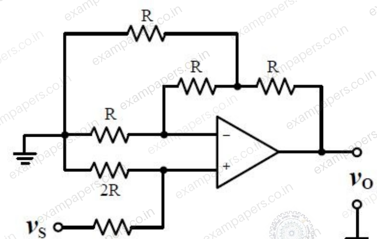
Which one of the following is TRUE?
Your answerChoose one option.
Log in to check the answer
You can attempt this question now. Sign in to view the answer key, explanations and discussion.Log in to check answerQuestion 49
Open questionEE-2NAT2 marksNeeds review
For the synchronous sequential circuit shown below, the output Z is zero for the initial conditions
.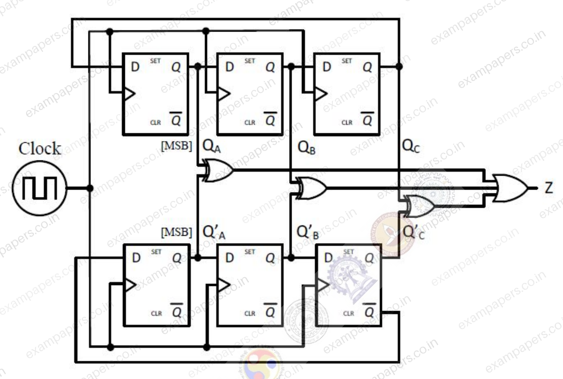
The minimum number of clock cycles after which the output Z would again become zero is __________
Log in to check the answer
You can attempt this question now. Sign in to view the answer key, explanations and discussion.Log in to check answerQuestion 52
Open questionEENAT2 marksNeeds review
The circuit shown in the figure uses matched transistors with a thermal voltage
mV. The base currents of the transistors are negligible. The value of the resistance R in
that is required to provide 1
A bias current for the differential amplifier block shown is
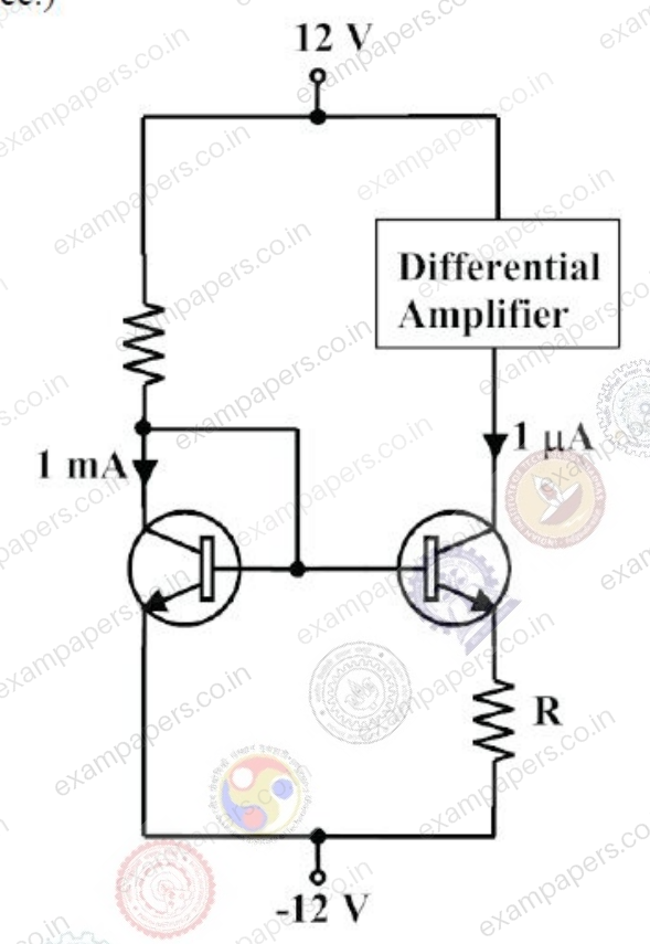
________. (Give the answer up to one decimal place.)
Log in to check the answer
You can attempt this question now. Sign in to view the answer key, explanations and discussion.Log in to check answer