
Electrical Engineering
GATE EE exam:gate PYQs
Build your understanding with focused practice from past exam papers.
Questions 41–50 of 715. Imported answers require independent review unless marked reviewed.
Question 41
Open questionEEMCQ2 marksNeeds review
A three-phase two-winding transformer has a voltage transformation ratio
, where
is the primary side voltage in p.u., and
is the secondary side voltage in p.u.
and
represent the currents injected into the primary and secondary sides of the transformer, respectively. The admittance corresponding to the leakage impedance of the transformer referred to the secondary is
p.u. Neglect the magnetizing branch. 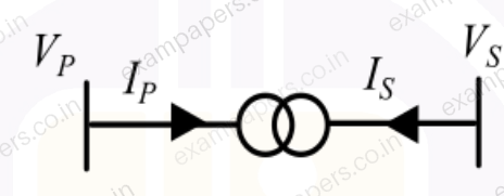
The Y bus representation of this transformer is:
Your answerChoose one option.
Log in to check the answer
You can attempt this question now. Sign in to view the answer key, explanations and discussion.Log in to check answerQuestion 42
Open questionEEMCQ2 marksNeeds review
An electrical component has voltage drop
, when the current through it is
. What is the average power dissipated over a half cycle corresponding to
?Your answerChoose one option.
Log in to check the answer
You can attempt this question now. Sign in to view the answer key, explanations and discussion.Log in to check answerQuestion 43
Open questionEEMCQ2 marksNeeds review
The electrical network shown has an independent voltage source (10 V) and a current source (1 u(t) mA).
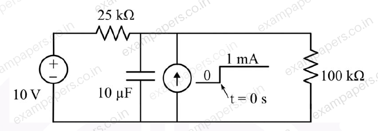
The voltage across the capacitor at time instants (in seconds)
,
, and
, respectively, is:Your answerChoose one option.
Log in to check the answer
You can attempt this question now. Sign in to view the answer key, explanations and discussion.Log in to check answerQuestion 44
Open questionEEMCQ2 marksNeeds review
The terminal voltage and current of a linear electrical network shown in Figure (a) are given in the table.
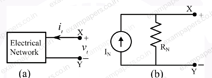
The correct choice for the parameters
of the Norton equivalent circuit shown in Figure (b) is:Your answerChoose one option.
Log in to check the answer
You can attempt this question now. Sign in to view the answer key, explanations and discussion.Log in to check answerQuestion 45
Open questionEEMCQ2 marksNeeds review
The digital circuit shown has 3 inputs (x, y, and z).
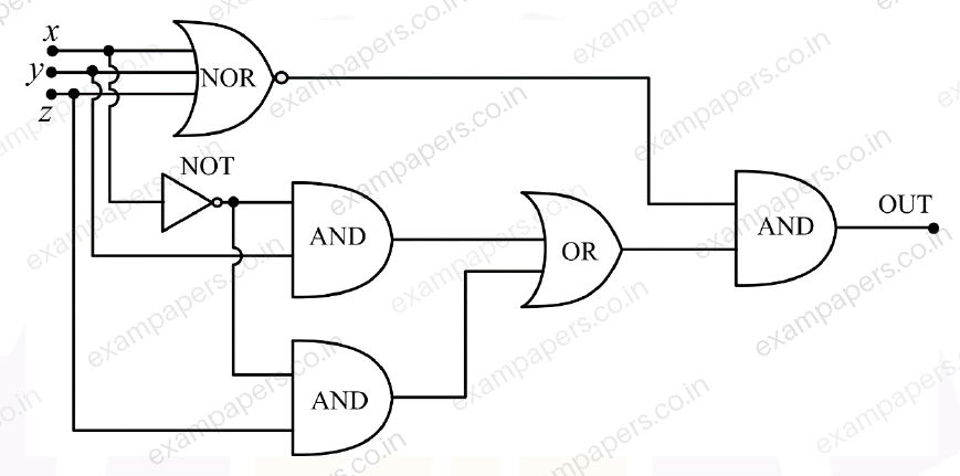
The simplified logical expression for the output (OUT) is:
Your answerChoose one option.
Log in to check the answer
You can attempt this question now. Sign in to view the answer key, explanations and discussion.Log in to check answerQuestion 46
Open questionEEMCQ2 marksNeeds review
The MOSFET switches shown in the circuit are ideal.
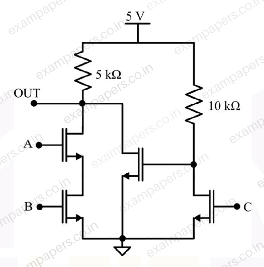
Which of the following is the correct option for Boolean logic expression of the output (OUT), and the maximum possible power (P) consumed by the circuit?
Your answerChoose one option.
Log in to check the answer
You can attempt this question now. Sign in to view the answer key, explanations and discussion.Log in to check answerQuestion 47
Open questionEEMCQ2 marksNeeds review
Consider the single-phase voltage source inverter circuit feeding an inductive load (L). Assume that the power MOSFET switches are ideal. S₁ and S₂ are switched on during the first 10 μs, and S₃ and S₄ are switched on during the next 10 μs in a switching cycle. The switches in the same leg are thus switched in a complementary fashion. Neglect the dead time. The waveform of the inductor current (i_L) in the steady state is triangular with a peak value of 5 A as shown.
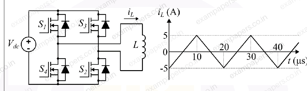
The rms value of the current through the switch S₁ is:
Your answerChoose one option.
Log in to check the answer
You can attempt this question now. Sign in to view the answer key, explanations and discussion.Log in to check answerQuestion 48
Open questionEEMCQ2 marksNeeds review
Consider the boost converter circuit shown. Assume that the semiconductor devices are ideal. In steady state, the inductor current rises linearly from 0 A to 6 A in the first 10
and then falls linearly from 6 A to 0 A in the next 10
of every switching cycle as shown. The load resistance R is 10
and the capacitance C is 500
. 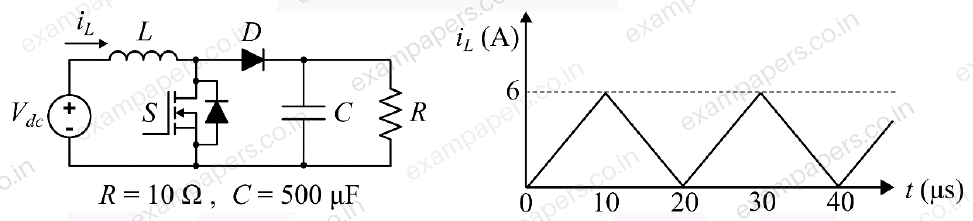
Neglect the ripple in the output voltage. What is the input voltage
?Your answerChoose one option.
Log in to check the answer
You can attempt this question now. Sign in to view the answer key, explanations and discussion.Log in to check answerQuestion 49
Open questionEEMCQ2 marksNeeds review
Which one of the following statements is ALWAYS correct about a collection of
column vectors, each having
real-valued entries?Your answerChoose one option.
Log in to check the answer
You can attempt this question now. Sign in to view the answer key, explanations and discussion.Log in to check answerQuestion 50
Open questionEEMCQ2 marksNeeds review
Consider the second-order differential equation
with initial conditions
The solution is given byYour answerChoose one option.
Log in to check the answer
You can attempt this question now. Sign in to view the answer key, explanations and discussion.Log in to check answer