
Electrical Engineering
GATE EE Power Electronics PYQs
Build your understanding with focused practice from past exam papers.
How to practice Power Electronics
Attempt a question, record the concept and assumptions, then check the available answer. Rework mistakes after revising the relevant concepts. Topic tags can overlap; review the question context.
Questions 1–10 of 66. Imported answers require independent review unless marked reviewed.
Question 27
Open questionEEMCQ1 markNeeds review
The figure shows a straight-line approximation for the forward characteristics of a power diode. A continuous on-state current of 15 A is flowing through the diode.
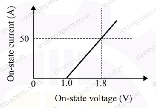
What is the power loss in the diode?
Your answerChoose one option.
Log in to check the answer
You can attempt this question now. Sign in to view the answer key, explanations and discussion.Log in to check answerQuestion 28
Open questionEEMCQ1 markNeeds review
Consider the circuit shown in Figure (a). A gate pulse
is applied between time instants
and
. After
, during the MOSFET turn OFF process, it experiences a voltage overshoot.Based on the
waveforms shown in Figure (b), which one of the following options is correct? 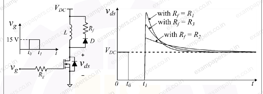
Your answerChoose one option.
Log in to check the answer
You can attempt this question now. Sign in to view the answer key, explanations and discussion.Log in to check answerQuestion 34
Open questionEENAT1 markNeeds review
Consider the circuit shown. Assume that the diode D is ideal. The supply voltage
V,
, and
. The peak diode current (in amperes) is ______________(Round off to one decimal place)

Log in to check the answer
You can attempt this question now. Sign in to view the answer key, explanations and discussion.Log in to check answerQuestion 47
Open questionEEMCQ2 marksNeeds review
Consider the single-phase voltage source inverter circuit feeding an inductive load (L). Assume that the power MOSFET switches are ideal. S₁ and S₂ are switched on during the first 10 μs, and S₃ and S₄ are switched on during the next 10 μs in a switching cycle. The switches in the same leg are thus switched in a complementary fashion. Neglect the dead time. The waveform of the inductor current (i_L) in the steady state is triangular with a peak value of 5 A as shown.
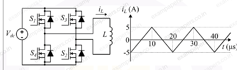
The rms value of the current through the switch S₁ is:
Your answerChoose one option.
Log in to check the answer
You can attempt this question now. Sign in to view the answer key, explanations and discussion.Log in to check answerQuestion 48
Open questionEEMCQ2 marksNeeds review
Consider the boost converter circuit shown. Assume that the semiconductor devices are ideal. In steady state, the inductor current rises linearly from 0 A to 6 A in the first 10
and then falls linearly from 6 A to 0 A in the next 10
of every switching cycle as shown. The load resistance R is 10
and the capacitance C is 500
. 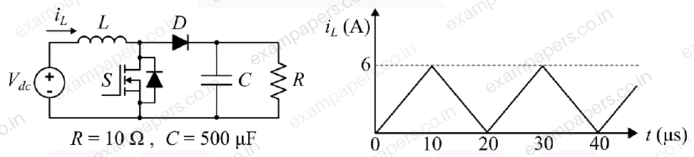
Neglect the ripple in the output voltage. What is the input voltage
?Your answerChoose one option.
Log in to check the answer
You can attempt this question now. Sign in to view the answer key, explanations and discussion.Log in to check answerQuestion 61
Open questionEENAT2 marksNeeds review
Consider the circuit shown. Assume that the diode (D) is ideal.

Given
V,
V, and
, the average value of the current through the diode is __________ A (Round off to two decimal places)Log in to check the answer
You can attempt this question now. Sign in to view the answer key, explanations and discussion.Log in to check answerQuestion 27
Open questionEEMCQ1 markNeeds review
The input voltage
and current
of a converter are given by,
where,
. The input power factor of the converter is closest toYour answerChoose one option.
Log in to check the answer
You can attempt this question now. Sign in to view the answer key, explanations and discussion.Log in to check answerQuestion 34
Open questionEENAT1 markNeeds review
In the circuit with ideal devices, the power MOSFET is operated with a duty cycle of 0.4 in a switching cycle with
and
. The power delivered by the current source, in W, is __________ (round off to the nearest integer). 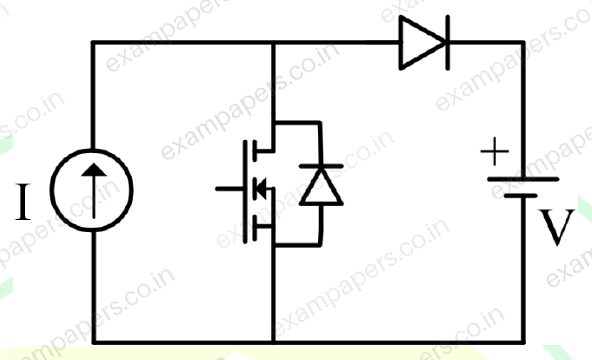
Log in to check the answer
You can attempt this question now. Sign in to view the answer key, explanations and discussion.Log in to check answerQuestion 46
Open questionEEMCQ2 marksNeeds review
The 3-phase modulating waveforms
and
, used in sinusoidal PWM in a Voltage Source Inverter (VSI) are
where
is the fundamental frequency. The modulating waveforms are compared with a 10 kHz triangular carrier whose magnitude varies between +1 and −1. The VSI has a DC link voltage of 600 V and feeds a star connected motor. The per phase fundamental RMS motor voltage, in volts, is closest toYour answerChoose one option.
Log in to check the answer
You can attempt this question now. Sign in to view the answer key, explanations and discussion.Log in to check answerQuestion 47
Open questionEEMCQ2 marksNeeds review
An ideal sinusoidal voltage source
feeds an ideal inductor
through an ideal SCR with firing angle
. If
, then the peak of the inductor current, in ampere, is closest to
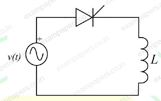
Your answerChoose one option.
Log in to check the answer
You can attempt this question now. Sign in to view the answer key, explanations and discussion.Log in to check answer