
Electrical Engineering
GATE EE topic:analog-and-digital-electronics PYQs
Build your understanding with focused practice from past exam papers.
Questions 41–50 of 57. Imported answers require independent review unless marked reviewed.
Question 35
Open questionEEMCQ2 marksNeeds review
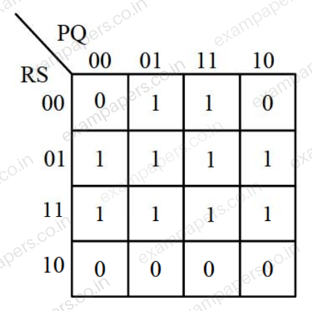
The output expression for the Karnaugh map shown below is
Your answerChoose one option.
Log in to check the answer
You can attempt this question now. Sign in to view the answer key, explanations and discussion.Log in to check answerQuestion 36
Open questionEEMCQ2 marksNeeds review
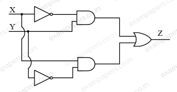
In the circuit shown below, X and Y are digital inputs, and Z is a digital output. The equivalent circuit is a
Your answerChoose one option.
Log in to check the answer
You can attempt this question now. Sign in to view the answer key, explanations and discussion.Log in to check answerQuestion 14
Open questionEEMCQ1 markNeeds review
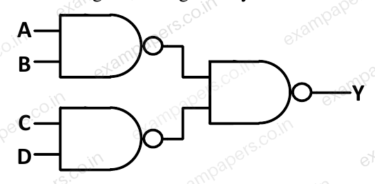
In the logic circuit shown in the figure, Y is given by
Your answerChoose one option.
Log in to check the answer
You can attempt this question now. Sign in to view the answer key, explanations and discussion.Log in to check answerQuestion 15
Open questionEEMCQ1 markNeeds review
The op-amp shown in the figure is ideal. The input impedance
is given by 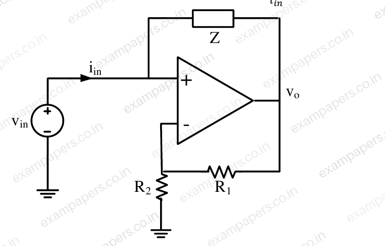
Your answerChoose one option.
Log in to check the answer
You can attempt this question now. Sign in to view the answer key, explanations and discussion.Log in to check answerQuestion 36
Open questionEEMCQ2 marksNeeds review
Which one of the following statements is true about the digital circuit shown in the figure
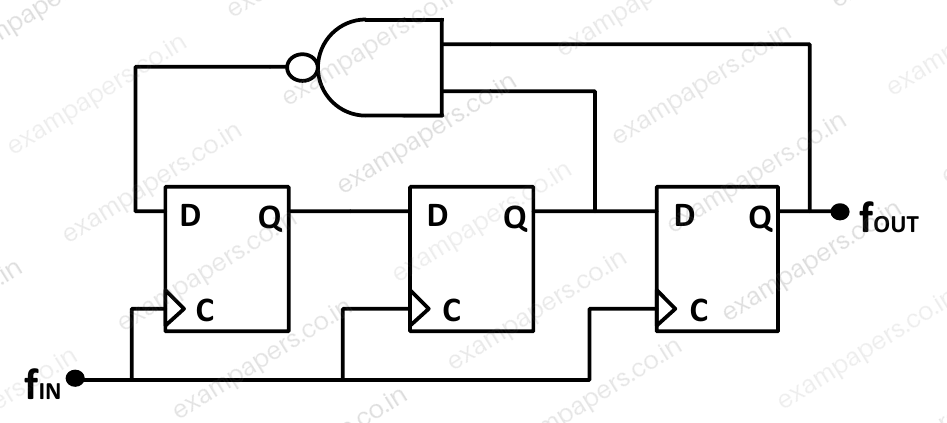
Your answerChoose one option.
Log in to check the answer
You can attempt this question now. Sign in to view the answer key, explanations and discussion.Log in to check answerQuestion 37
Open questionEEMCQ2 marksNeeds review
Digital input signals
,
,
with
as the MSB and
as the LSB are used to realize the Boolean function
, where
denotes the
minterm. In addition,
has a don’t care for
. The simplified expression for
is given byYour answerChoose one option.
Log in to check the answer
You can attempt this question now. Sign in to view the answer key, explanations and discussion.Log in to check answerQuestion 41
Open questionEENAT2 marksNeeds review
In the circuit shown in the figure, the bipolar junction transistor (BJT) has a current gain
. The base-emitter voltage drop is a constant,
. The value of the Thevenin equivalent resistance
(in
) as shown in the figure 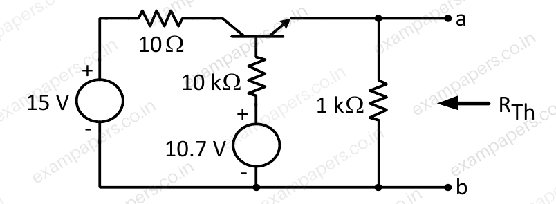
is ______ (up to 2 decimal places).
Log in to check the answer
You can attempt this question now. Sign in to view the answer key, explanations and discussion.Log in to check answerQuestion 10
Open questionEE-2MCQ1 markNeeds review
For a 3-input logic circuit shown below, the output
can be expressed as 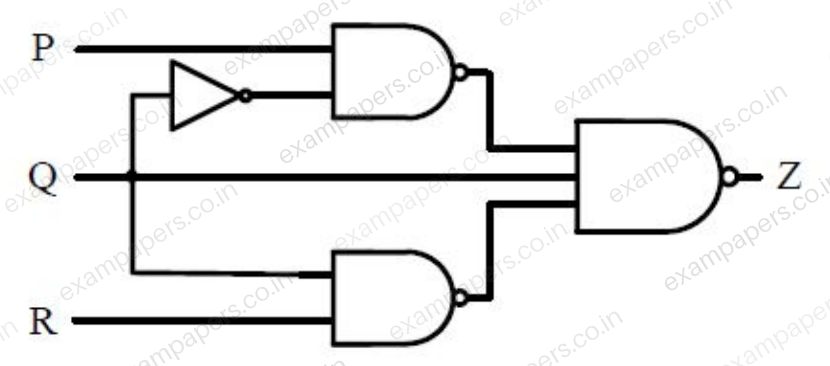
Your answerChoose one option.
Log in to check the answer
You can attempt this question now. Sign in to view the answer key, explanations and discussion.Log in to check answerQuestion 13
Open questionEEMCQ1 markNeeds review
The Boolean expression
simplifies toYour answerChoose one option.
Log in to check the answer
You can attempt this question now. Sign in to view the answer key, explanations and discussion.Log in to check answerQuestion 14
Open questionEEMCQ1 markNeeds review
For the circuit shown in the figure below, assume that diodes D₁, D₂ and D₃ are ideal.
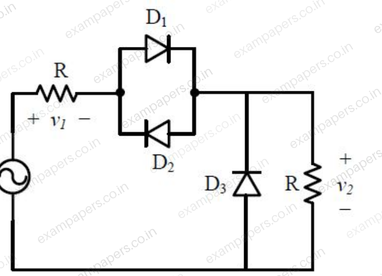
The DC components of voltages
and
, respectively areYour answerChoose one option.
Log in to check the answer
You can attempt this question now. Sign in to view the answer key, explanations and discussion.Log in to check answer