
Instrumentation Engineering
GATE IN Analog Electronics PYQs
Build your understanding with focused practice from past exam papers.
Questions 11–20 of 65. Imported answers require independent review unless marked reviewed.
Question 24
Open questionINNAT1 markNeeds review
Figure shows an amplifier using an NMOS transistor. Assume that the transistor is in saturation with device parameters,
, threshold voltage
and
. Ignore the channel length modulation effect. The drain current of the transistor at the operating point is ______ μA (rounded off to nearest integer). 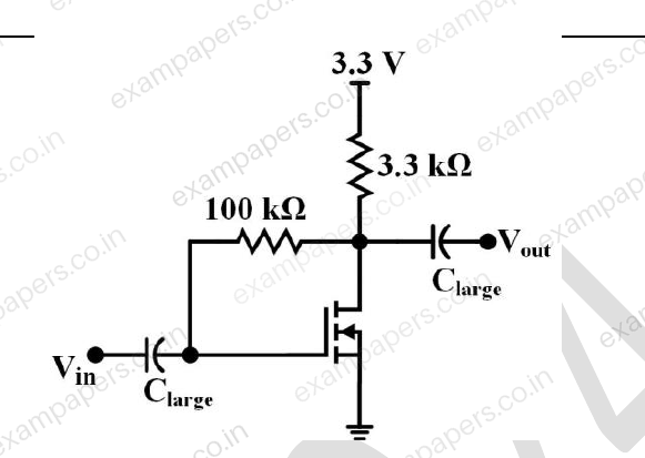
Log in to check the answer
You can attempt this question now. Sign in to view the answer key, explanations and discussion.Log in to check answerQuestion 41
Open questionINMCQ2 marksNeeds review
In the figure shown, both the opamps A₁ and A₂ are ideal, except that the opamp A₁ has an offset voltage (
) of 1 mV. For
V, the values of the output voltages
and
, respectively, are 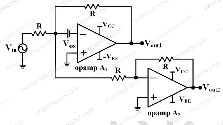
Your answerChoose one option.
Log in to check the answer
You can attempt this question now. Sign in to view the answer key, explanations and discussion.Log in to check answerQuestion 43
Open questionINMCQ2 marksNeeds review
In the figure shown, R = 1 kΩ and C = 0.1 μF. For a dc gain of −10, the 3 dB cut-off frequency (rounded off to one decimal place) is
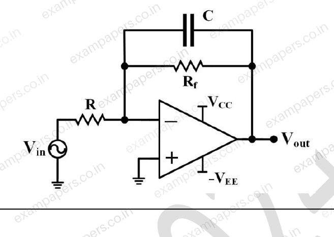
Assume the opamp is ideal.
Your answerChoose one option.
Log in to check the answer
You can attempt this question now. Sign in to view the answer key, explanations and discussion.Log in to check answerQuestion 51
Open questionINNAT2 marksNeeds review
In the figure shown,
,
, and INA is assumed to be ideal. The equivalent resistance between A and B is ____ k
(rounded off to nearest integer). 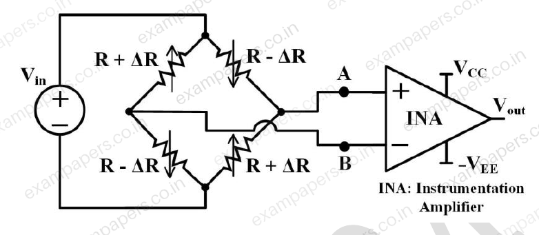
Log in to check the answer
You can attempt this question now. Sign in to view the answer key, explanations and discussion.Log in to check answerQuestion 52
Open questionINNAT2 marksNeeds review
Consider the capacitive sensor circuit and its output voltage shown in the figure. The circuit is switched ON at
. Assuming the opamp to be ideal, the frequency of the output voltage
is __________ kHz (rounded off to two decimal places). 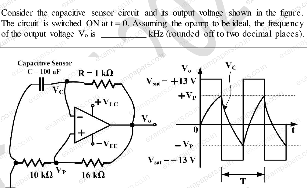
Log in to check the answer
You can attempt this question now. Sign in to view the answer key, explanations and discussion.Log in to check answerQuestion 57
Open questionINNAT2 marksNeeds review
In the figure shown, the diode current is given by
. V_D is the diode voltage in volts, T is the absolute temperature in Kelvin, α = 1.16 × 10⁴ K/V, and I_S = 10⁻¹⁵ A is the saturation current. The dc current source, opamp and the resistors are ideal, and are assumed to be temperature independent. The change in the output voltage (V_out) per Kelvin change in temperature is ________ mV (rounded off to one decimal place). 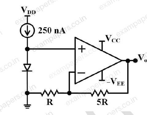
Log in to check the answer
You can attempt this question now. Sign in to view the answer key, explanations and discussion.Log in to check answerQuestion 59
Open questionINNAT2 marksNeeds review
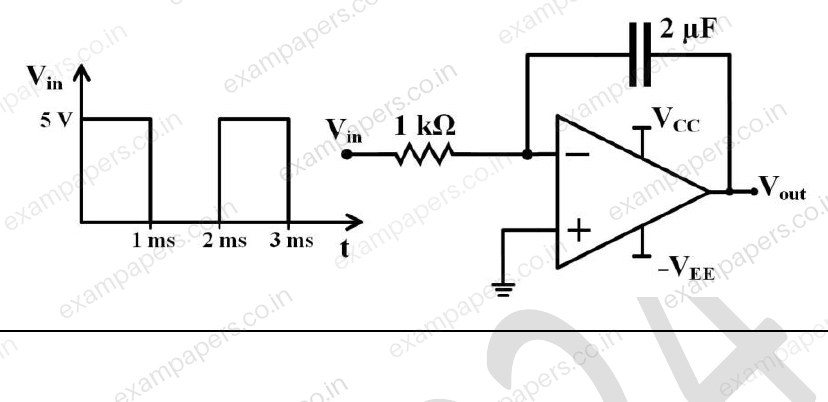
In the circuit shown, assume the opamp is ideal and the initial charge on the capacitor is zero. The output voltage at time t = 2 ms is ____ V (rounded off to one decimal place).
Log in to check the answer
You can attempt this question now. Sign in to view the answer key, explanations and discussion.Log in to check answerQuestion 26
Open questionINNAT1 markNeeds review
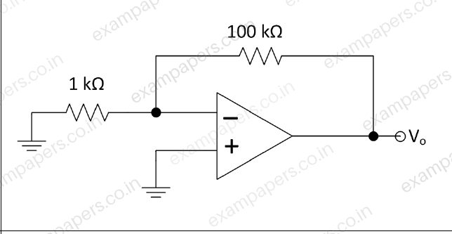
The opamp in the circuit shown is ideal, except that it has an input bias current of 1 nA and an input offset voltage of 10 μV. The resulting worst-case output voltage will be ±_____ μV (rounded off to the nearest integer).
Log in to check the answer
You can attempt this question now. Sign in to view the answer key, explanations and discussion.Log in to check answerQuestion 56
Open questionINNAT2 marksNeeds review
The figure below shows a feedback amplifier constructed using an nMOS transistor. Assume that
mA/V
, threshold voltage
V and W/L = 2. The bias voltage at the drain terminal is 4 V. The capacitors
offer zero impedance at the signal frequency. The ratio
is ____________(rounded off to two decimal places). 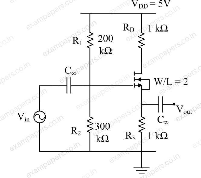
Log in to check the answer
You can attempt this question now. Sign in to view the answer key, explanations and discussion.Log in to check answerQuestion 59
Open questionINNAT2 marksNeeds review
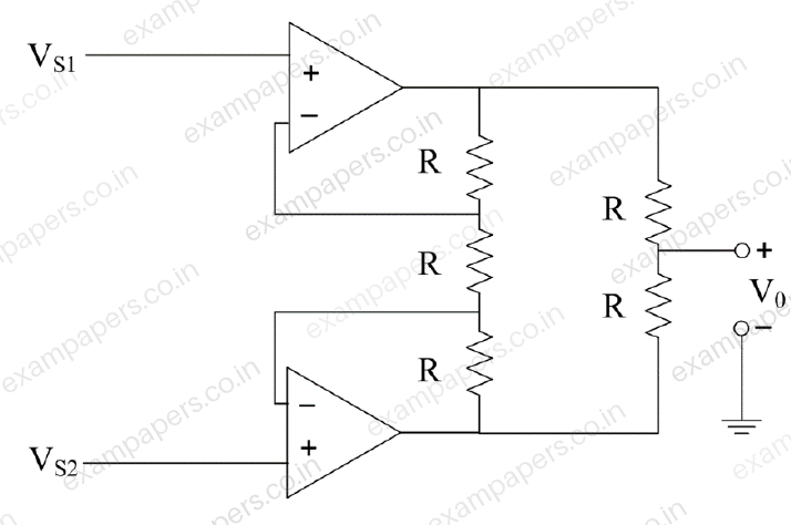
The opamps in the circuit are ideal. The input signals are
V and
V. The average value of the voltage
is _____ V (rounded off to two decimal places).
Log in to check the answer
You can attempt this question now. Sign in to view the answer key, explanations and discussion.Log in to check answer