
Instrumentation Engineering
GATE IN Digital Electronics PYQs
Build your understanding with focused practice from past exam papers.
Questions 21–30 of 57. Imported answers require independent review unless marked reviewed.
Question 41
Open questionINMCQ2 marksNeeds review
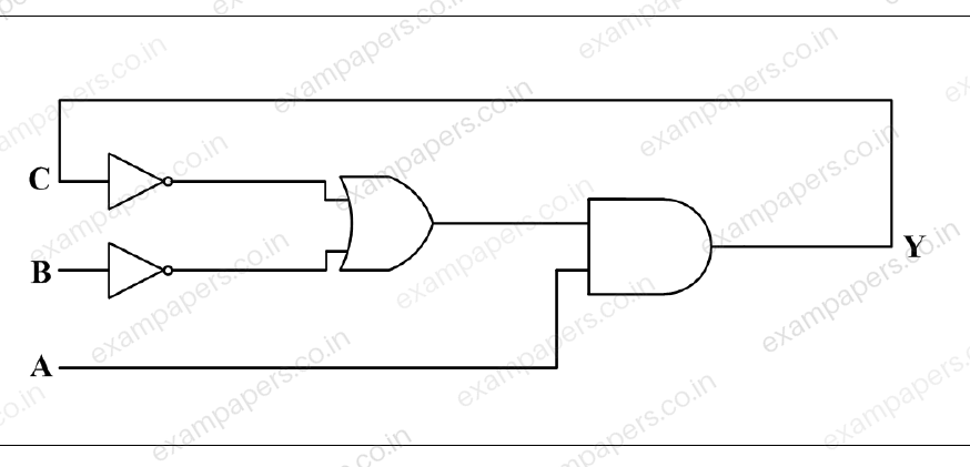
For the given digital circuit, A = B = 1. Assume that AND, OR, and NOT gates have propagation delays of 10 ns, 10 ns, and 5 ns respectively. All lines have zero propagation delay. Given that C = 1 when the circuit is turned on, the frequency of steady-state oscillation of the output Y is _____.
Your answerChoose one option.
Log in to check the answer
You can attempt this question now. Sign in to view the answer key, explanations and discussion.Log in to check answerQuestion 42
Open questionINMCQ2 marksNeeds review
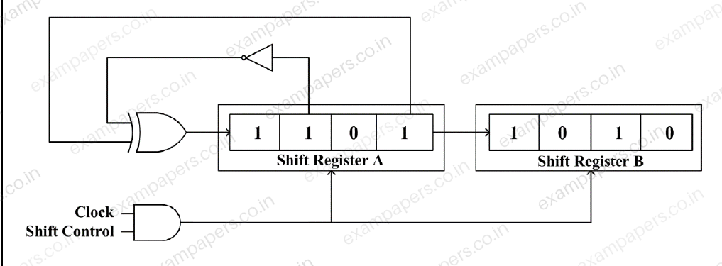
In the circuit shown, the initial binary content of shift register A is 1101 and that of shift register B is 1010. The shift registers are positive-edge triggered, and the gates have no delay.
When the shift control is high, what will be the binary content of the shift registers A and B after four clock pulses?
Your answerChoose one option.
Log in to check the answer
You can attempt this question now. Sign in to view the answer key, explanations and discussion.Log in to check answerQuestion 21
Open questionINMCQ1 markNeeds review
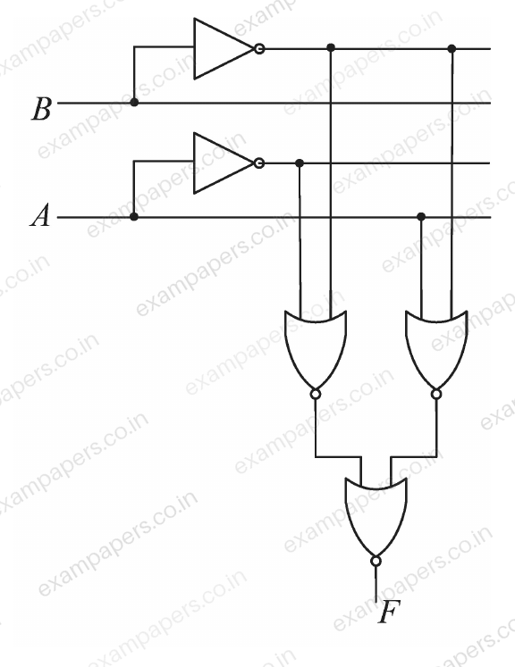
The logic block shown has an output
given by ______
Your answerChoose one option.
Log in to check the answer
You can attempt this question now. Sign in to view the answer key, explanations and discussion.Log in to check answerQuestion 23
Open questionINMSQ1 markNeeds review
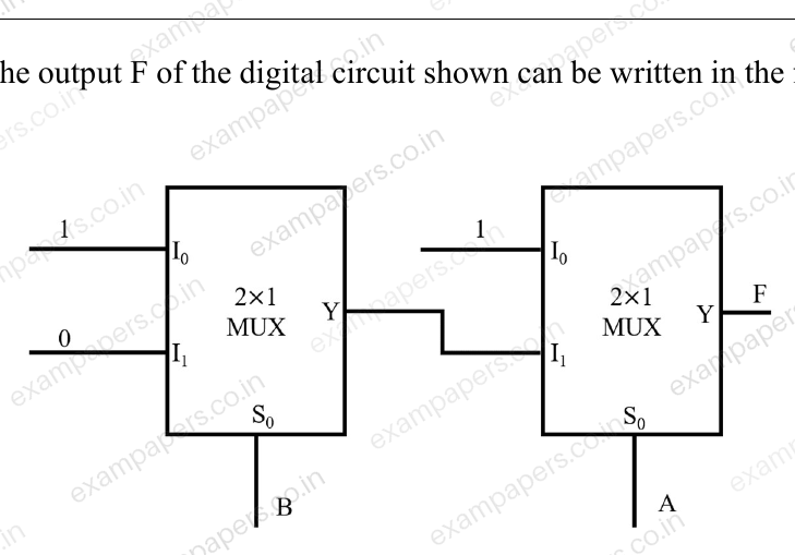
The output F of the digital circuit shown can be written in the form(s) ______
Your answerSelect all correct options. You can choose more than one.
Log in to check the answer
You can attempt this question now. Sign in to view the answer key, explanations and discussion.Log in to check answerQuestion 25
Open questionINNAT1 markNeeds review
An analog-to-digital converter with resolution 0.01 V converts analog signals between 0 V to +10 V to an unsigned binary output. The minimum number of bits (in integer) in the output is ______
Log in to check the answer
You can attempt this question now. Sign in to view the answer key, explanations and discussion.Log in to check answerQuestion 42
Open questionINMCQ2 marksNeeds review
A resistor ladder digital-to-analog converter (DAC) receives a digital input that results in the circuit having the state as shown in the figure. For this digital input, the Thevenin voltage,
, and Thevenin resistance,
, as seen at the output node are ________ 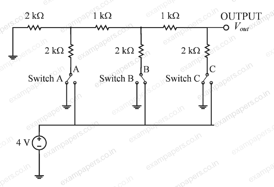
Your answerChoose one option.
Log in to check the answer
You can attempt this question now. Sign in to view the answer key, explanations and discussion.Log in to check answerQuestion 46
Open questionINMCQ2 marksNeeds review
The digital circuit shown ______
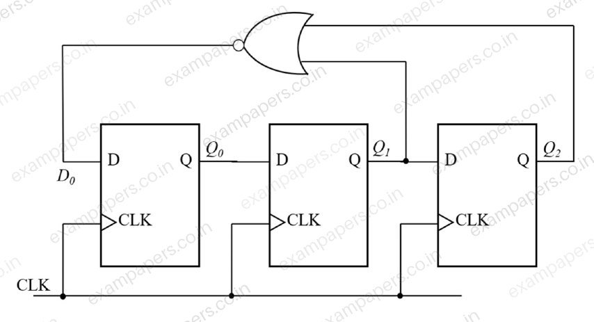
Your answerChoose one option.
Log in to check the answer
You can attempt this question now. Sign in to view the answer key, explanations and discussion.Log in to check answerQuestion 48
Open questionINMCQ2 marksNeeds review
and
are two 2-bit unsigned binary numbers. If
is a Boolean function such that
only when
, and
otherwise, then
can be minimized to the form ______Your answerChoose one option.
Log in to check the answer
You can attempt this question now. Sign in to view the answer key, explanations and discussion.Log in to check answerQuestion 10
Open questionINMSQ1 markNeeds review
For a 4-bit Flash type Analog to Digital Convertor (ADC) with full scale input voltage range “V”, which of the following statement(s) is/are true?
Your answerSelect all correct options. You can choose more than one.
Log in to check the answer
You can attempt this question now. Sign in to view the answer key, explanations and discussion.Log in to check answerQuestion 11
Open questionINMSQ1 markNeeds review
A 16-bit microprocessor has twenty address lines (
to
) and 16 data lines. The higher eight significant lines of the data bus of the processor are tied to the 8-data lines of a 16 Kbyte memory that can store one byte in each of its 16K address locations. The memory chip should map onto contiguous memory locations and occupy only 16 Kbyte of memory space. Which of the following statement(s) is/are correct with respect to the above design:Your answerSelect all correct options. You can choose more than one.
Log in to check the answer
You can attempt this question now. Sign in to view the answer key, explanations and discussion.Log in to check answer