
Instrumentation Engineering
GATE IN topic:analog-electronics PYQs
Build your understanding with focused practice from past exam papers.
Questions 21–30 of 65. Imported answers require independent review unless marked reviewed.
Question 60
Open questionINNAT2 marksNeeds review
In the circuit shown, the input voltage
mV. The switch and the opamp are ideal. At time
, the initial charge stored in the 10 nF capacitor is 1 nC, with the polarity as indicated in the figure. The switch S is controlled using a 1 kHz square-wave voltage signal
as shown. Whenever
is ‘High’, S is in position ‘1’ and when
is ‘Low’, S is in position ‘2’.
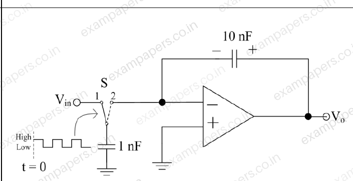
At
ms, the magnitude of the voltage
will be ______ mV (rounded off to the nearest integer).Log in to check the answer
You can attempt this question now. Sign in to view the answer key, explanations and discussion.Log in to check answerQuestion 62
Open questionINNAT2 marksNeeds review
In the circuit shown, assuming an ideal opamp, the value of the output voltage
____ V (rounded off to one decimal place).
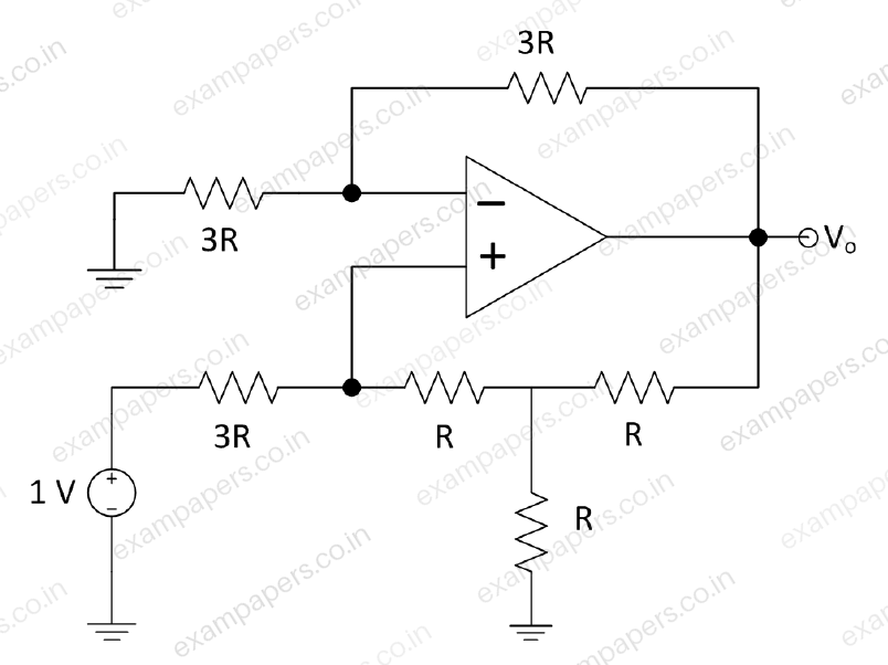
Log in to check the answer
You can attempt this question now. Sign in to view the answer key, explanations and discussion.Log in to check answerQuestion 31
Open questionINNAT1 markNeeds review
A Zener diode is used as a 4 V voltage regulator in the circuit shown. Given that the diode requires a minimum current of 4 mA for voltage regulation, the maximum current (in milliamperes) permitted to flow through the load
is ______ (round off to one decimal place)
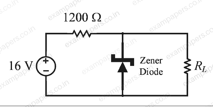
Log in to check the answer
You can attempt this question now. Sign in to view the answer key, explanations and discussion.Log in to check answerQuestion 35
Open questionINNAT1 markNeeds review
An OPAMP has a gain of
, an input impedance of 10 M
and an output impedance of 100
. The OPAMP is used in unity-gain feedback configuration in a voltage buffer circuit. The closed-loop output impedance of the OPAMP (in milliohms) in the circuit is ________ (round off to one decimal place)Log in to check the answer
You can attempt this question now. Sign in to view the answer key, explanations and discussion.Log in to check answerQuestion 36
Open questionINMCQ2 marksNeeds review
A signal
shown is applied from
to
to the circuit shown. Given the initial voltage across the capacitor is 0.3 V, and that the diode is ideal, the open circuit voltage
at
is ________ 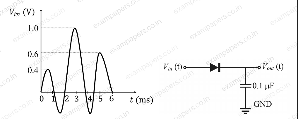
Your answerChoose one option.
Log in to check the answer
You can attempt this question now. Sign in to view the answer key, explanations and discussion.Log in to check answerQuestion 44
Open questionINMCQ2 marksNeeds review
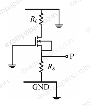
In the small signal circuit shown, the enhancement mode n-channel MOSFET is biased in saturation with transconductance
. If channel length modulation is ignored, the small signal impedance looking into the node P is given by ______
Your answerChoose one option.
Log in to check the answer
You can attempt this question now. Sign in to view the answer key, explanations and discussion.Log in to check answerQuestion 47
Open questionINMCQ2 marksNeeds review
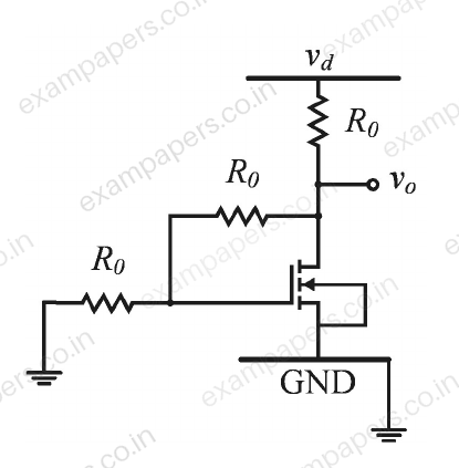
In the small signal circuit shown, the enhancement mode n-channel MOSFET is biased in saturation with a transconductance
. A small signal low-frequency voltage
injected at the supply terminal results in a small signal voltage
at the output. If the channel length modulation of the MOSFET is ignored, the small signal gain
is given by ______
Your answerChoose one option.
Log in to check the answer
You can attempt this question now. Sign in to view the answer key, explanations and discussion.Log in to check answerQuestion 56
Open questionINNAT2 marksNeeds review
The circuit shown is driven by a sinusoidal input voltage,
, resulting in the output voltage,
. The frequency (in kilohertz) at which the voltage gain is 0 dB is ______ (round off to two decimal places) 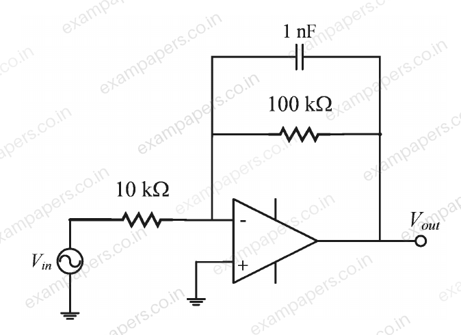
Log in to check the answer
You can attempt this question now. Sign in to view the answer key, explanations and discussion.Log in to check answerQuestion 58
Open questionINNAT2 marksNeeds review
In the circuit shown,
and
. If the base-to-emitter voltage of the npn BJT is 0.7 V and the collector-to-emitter voltage is 5.2 V, the
(current gain) of the BJT is ______ (round off to two decimal places) 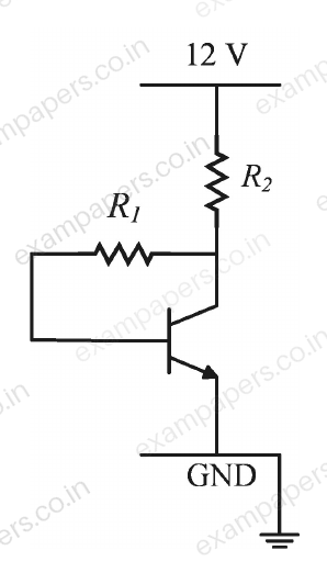
Log in to check the answer
You can attempt this question now. Sign in to view the answer key, explanations and discussion.Log in to check answerQuestion 64
Open questionINNAT2 marksNeeds review
In the circuit shown, the switch is initially closed. It is opened at
and remains open thereafter. The time (in milliseconds) at which the output voltage
becomes LOW is ______ (round off to three decimal places) 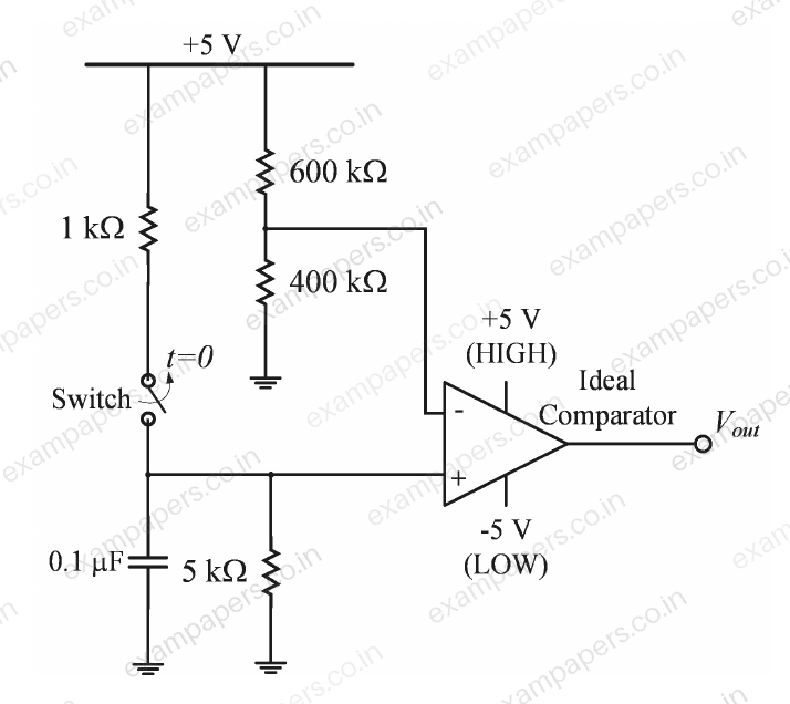
Log in to check the answer
You can attempt this question now. Sign in to view the answer key, explanations and discussion.Log in to check answer