
Physics
GATE PH Electronics PYQs
Build your understanding with focused practice from past exam papers.
How to practice Electronics
Attempt a question, record the concept and assumptions, then check the available answer. Rework mistakes after revising the relevant concepts. Topic tags can overlap; review the question context.
Questions 1–10 of 40. Imported answers require independent review unless marked reviewed.
Question 18
Open questionPHMCQ1 markNeeds review
The symbols C, D,
and
shown in the figure denote capacitor, ideal diode, input voltage and output voltage, respectively.
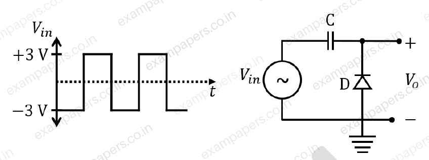
Which one of the following output waveforms (
) is correct for the given input waveform (
)?Your answerChoose one option.
Log in to check the answer
You can attempt this question now. Sign in to view the answer key, explanations and discussion.Log in to check answerQuestion 24
Open questionPHMCQ1 markNeeds review
Consider the following circuit:
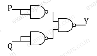
Suppose the input signal
is
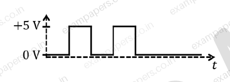
and the input signal
is
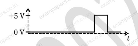
Which one of the following output signals is correct?
Your answerChoose one option.
Log in to check the answer
You can attempt this question now. Sign in to view the answer key, explanations and discussion.Log in to check answerQuestion 32
Open questionPHNAT1 markNeeds review
The minimum number of basic logic gates required to realize the Boolean expression
is ____ (in integer).Log in to check the answer
You can attempt this question now. Sign in to view the answer key, explanations and discussion.Log in to check answerQuestion 50
Open questionPHMSQ2 marksNeeds review
An extrinsic semiconductor shown in figure carries a current of 2 mA along its length parallel to +x axis.
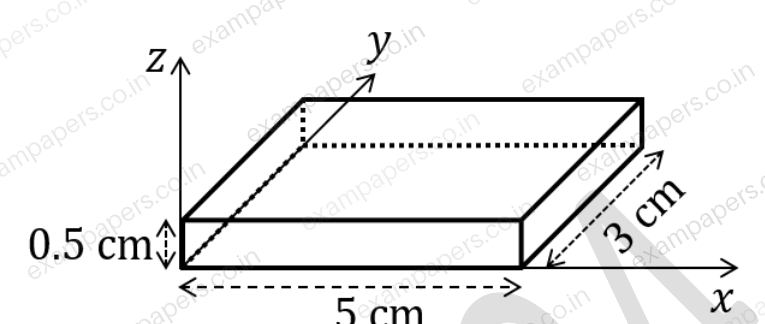
When the majority charge carrier concentration is
and the sample is exposed to a constant magnetic field applied along the +z direction, a Hall voltage of 20 mV is measured with the negative polarity at
plane. Take the electric charge as
C. The concentration of minority charge carrier is negligible. Which of the following statement is/are true?Your answerSelect all correct options. You can choose more than one.
Log in to check the answer
You can attempt this question now. Sign in to view the answer key, explanations and discussion.Log in to check answerQuestion 58
Open questionPHNAT2 marksNeeds review
A typical biasing of a silicon transistor is shown in figure.
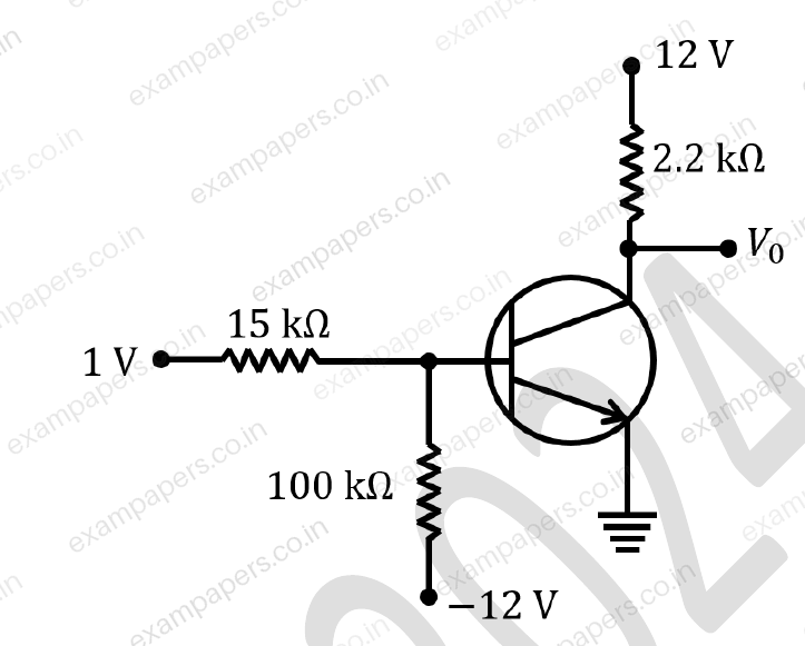
The value of common-emitter current gain
for the transistor is 100. Ignore reverse saturation current. The output voltage
(in V) is ______ (in integer).Log in to check the answer
You can attempt this question now. Sign in to view the answer key, explanations and discussion.Log in to check answerQuestion 63
Open questionPHNAT2 marksNeeds review
Consider the operational amplifier circuit shown in figure.
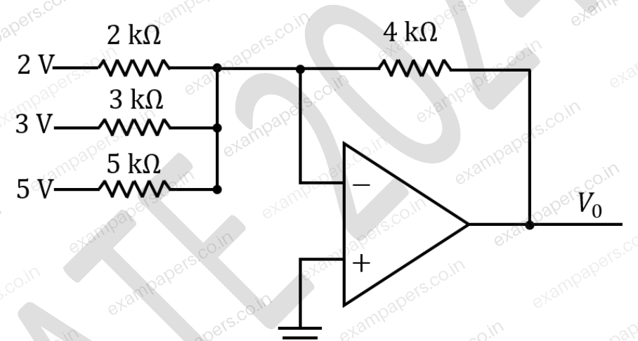
The output voltage
is ______ V (in integer).Log in to check the answer
You can attempt this question now. Sign in to view the answer key, explanations and discussion.Log in to check answerQuestion 13
Open questionPHMCQ1 markNeeds review
Choose the most appropriate matching of the items in Column 1 with those in Column 2.
Column 1 | Column 2 |
|---|---|
(i) PIN diode | P. Voltage regulation |
(ii) Tunnel diode | Q. Radio frequency and microwave devices |
(iii) Zener diode | R. Optoelectronic detection |
(iv) Photo diode | S. Oscillator |
Your answerChoose one option.
Log in to check the answer
You can attempt this question now. Sign in to view the answer key, explanations and discussion.Log in to check answerQuestion 24
Open questionPHMCQ1 markNeeds review
Which one of the following options is CORRECT for the given logic circuit?
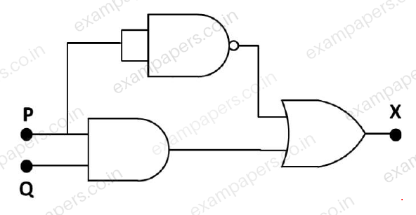
Your answerChoose one option.
Log in to check the answer
You can attempt this question now. Sign in to view the answer key, explanations and discussion.Log in to check answerQuestion 34
Open questionPHNAT1 markNeeds review
For a transistor amplifier, the frequency response is such that the mid band voltage gain is 200. The cutoff frequencies are 20 Hz and 20 kHz. What is the ratio (rounded off to two decimal places) of the voltage gain at 10 Hz to that at 100 kHz?
Log in to check the answer
You can attempt this question now. Sign in to view the answer key, explanations and discussion.Log in to check answerQuestion 37
Open questionPHMCQ2 marksNeeds review
An input voltage in the form of a square wave of frequency 1 kHz is given to a circuit, which results in the output shown schematically below. Which one of the following options is the CORRECT representation of the circuit?
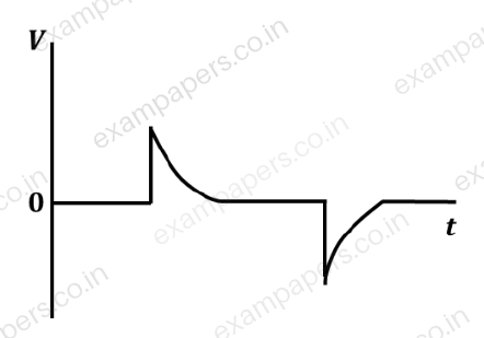
Your answerChoose one option.
Log in to check the answer
You can attempt this question now. Sign in to view the answer key, explanations and discussion.Log in to check answer