
Electrical Engineering
2017 · Paper 1
Take it one question at a time. Try an answer, then check your understanding.
Complete GATE EE 2017 Paper 1 overview, original pages and practice · Timed previous-paper practice
Questions 37–39 of 65. Imported answers require review unless explicitly marked reviewed.
Question 37
Open questionEEMCQ2 marksNeeds review
The logical gate implemented using the circuit shown below where, V₁ and V₂ are inputs (with 0 V as digital 0 and 5 V as digital 1) and Vₒᵤₜ is the output, is
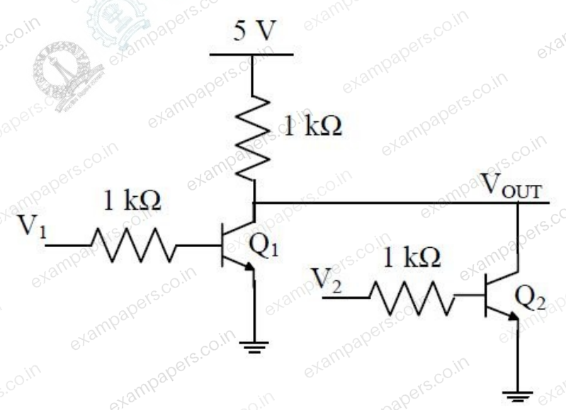
Your answerChoose one option.
Log in to check the answer
You can attempt this question now. Sign in to view the answer key, explanations and discussion.Log in to check answerQuestion 38
Open questionEEMCQ2 marksNeeds review
The input voltage V_DC of the buck-boost converter shown below varies from 32 V to 72 V. Assume that all components are ideal, inductor current is continuous, and output voltage is ripple free. The range of duty ratio D of the converter for which the magnitude of the steady-state output voltage remains constant at 48 V is
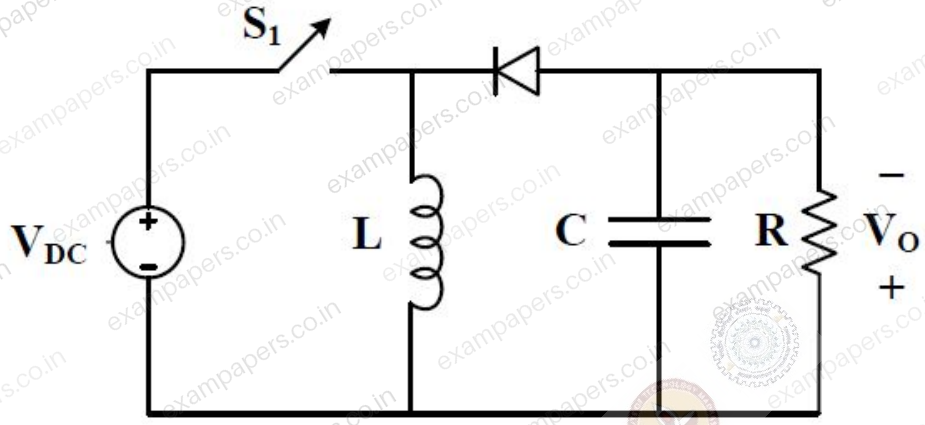
Your answerChoose one option.
Log in to check the answer
You can attempt this question now. Sign in to view the answer key, explanations and discussion.Log in to check answerQuestion 39
Open questionEEMCQ2 marksNeeds review
A load is supplied by a 230 V, 50 Hz source. The active power P and the reactive power Q consumed by the load are such that 1 kW ≤ P ≤ 2 kW and 1 kVAR ≤ Q ≤ 2 kVAR. A capacitor connected across the load for power factor correction generates 1 kVAR reactive power. The worst case power factor after power factor correction is
Your answerChoose one option.
Log in to check the answer
You can attempt this question now. Sign in to view the answer key, explanations and discussion.Log in to check answer