
Electronics and Communication Engineering
GATE ECE Carrier transport PYQs
Build your understanding with focused practice from past exam papers.
How to practice Carrier transport
Attempt a question, record the concept and assumptions, then check the available answer. Rework mistakes after revising the relevant concepts. Topic tags can overlap; review the question context.
Questions 1–10 of 17. Imported answers require independent review unless marked reviewed.
Question 14
Open questionECMCQ1 markNeeds review
Consider carrier transport in a Zener diode in the breakdown region. Which is the dominant transport mechanism for current flow in this case?
Your answerChoose one option.
Log in to check the answer
You can attempt this question now. Sign in to view the answer key, explanations and discussion.Log in to check answerQuestion 64
Open questionECNAT2 marksNeeds review
Consider that the concentration of electrons in a semiconductor bar varies linearly from
at
to
at
along the x-direction. Assume that the concentration of electrons is not varying along other directions (that is along y- and z-directions). [Given: the mobility of electron is
, thermal voltage is
and electron charge is
Coulomb.] The density of electron diffusion current (in A/mm
) is ___. (rounded off to two decimal places)Log in to check the answer
You can attempt this question now. Sign in to view the answer key, explanations and discussion.Log in to check answerQuestion 46
Open questionECMCQ2 marksNeeds review
The intrinsic carrier concentration of a semiconductor is 2.5 × 10¹⁶ /m³ at 300 K. If the electron and hole mobilities are 0.15 m²/Vs and 0.05 m²/Vs, respectively, then the intrinsic resistivity of the semiconductor (in kΩ.m) at 300 K is ______.
(Charge of an electron e = 1.6 × 10⁻¹⁹ C.)
Your answerChoose one option.
Log in to check the answer
You can attempt this question now. Sign in to view the answer key, explanations and discussion.Log in to check answerQuestion 48
Open questionECMCQ2 marksNeeds review
The electron mobility μₙ in a non-degenerate germanium semiconductor at 300 K is 0.38 m²/Vs.
The electron diffusivity Dₙ at 300 K (in cm²/s, rounded off to the nearest integer) is ______.
(Consider the Boltzmann constant kB = 1.38 × 10⁻²³ J/K and the charge of an electron e = 1.6 × 10⁻¹⁹ C.)
Your answerChoose one option.
Log in to check the answer
You can attempt this question now. Sign in to view the answer key, explanations and discussion.Log in to check answerQuestion 50
Open questionECMCQ2 marksNeeds review
An electric field of
is applied along the length of a copper wire of circular cross-section with diameter
. Copper has a conductivity of
.The current (in Amperes, rounded off to two decimal places) flowing through the wire is ______.
Your answerChoose one option.
Log in to check the answer
You can attempt this question now. Sign in to view the answer key, explanations and discussion.Log in to check answerQuestion 26
Open questionECMSQ1 markNeeds review
The free electron concentration profile
in a doped semiconductor at equilibrium is shown in the figure, where the points A, B, and C mark three different positions. Which of the following statements is/are true? 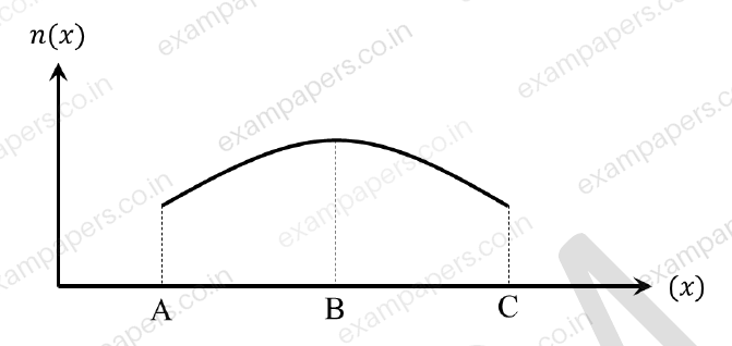
Your answerSelect all correct options. You can choose more than one.
Log in to check the answer
You can attempt this question now. Sign in to view the answer key, explanations and discussion.Log in to check answerQuestion 16
Open questionECMCQ1 markNeeds review
Consider a long rectangular bar of direct bandgap
-type semiconductor. The equilibrium hole density is
and the intrinsic carrier concentration is
. Electron and hole diffusion lengths are
and
, respectively.The left side of the bar (
) is uniformly illuminated with a laser having photon energy greater than the bandgap of the semiconductor. Excess electron-hole pairs are generated ONLY at
because of the laser. The steady state electron density at
is
due to laser illumination. Under these conditions and ignoring electric field, the closest approximation (among the given options) of the steady state electron density at
is _________.Your answerChoose one option.
Log in to check the answer
You can attempt this question now. Sign in to view the answer key, explanations and discussion.Log in to check answerQuestion 47
Open questionECMSQ2 marksNeeds review
Select the CORRECT statement(s) regarding semiconductor devices.
Your answerSelect all correct options. You can choose more than one.
Log in to check the answer
You can attempt this question now. Sign in to view the answer key, explanations and discussion.Log in to check answerQuestion 56
Open questionECNAT2 marksNeeds review
A
-type semiconductor with zero electric field is under illumination (low level injection) in steady state condition. Excess minority carrier density is zero at
, where
cm is the diffusion length for electrons. Assume electronic charge,
C. The profiles of photo-generation rate of carriers and the recombination rate of excess minority carriers (
) are shown. Under these conditions, the magnitude of the current density due to the photo-generated electrons at
is ________ mA/cm
(rounded off to two decimal places). 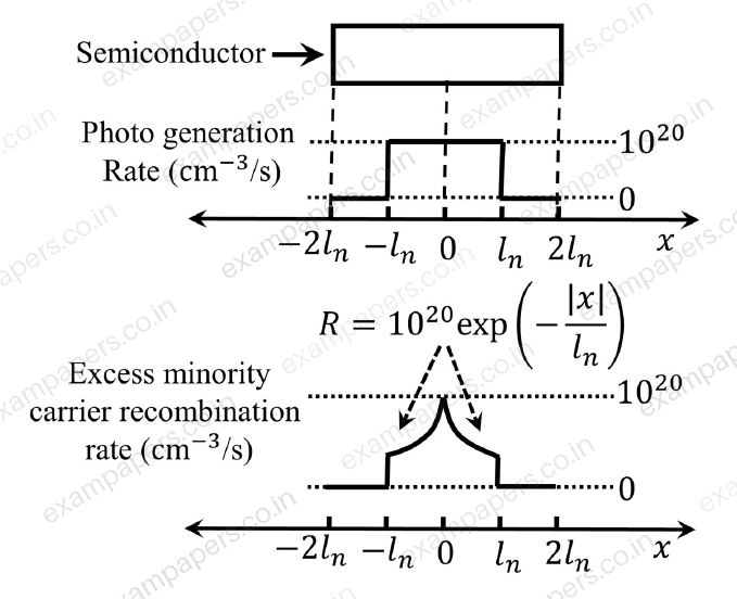
Log in to check the answer
You can attempt this question now. Sign in to view the answer key, explanations and discussion.Log in to check answerQuestion 9
Open questionECMCQ1 markNeeds review
A bar of Gallium Arsenide (GaAs) is doped with Silicon such that the Silicon atoms occupy Gallium and Arsenic sites in the GaAs crystal. Which one of the following statements is true?
Your answerChoose one option.
Log in to check the answer
You can attempt this question now. Sign in to view the answer key, explanations and discussion.Log in to check answer