
Electronics and Communication Engineering
GATE ECE Diode circuits PYQs
Build your understanding with focused practice from past exam papers.
How to practice Diode circuits
Attempt a question, record the concept and assumptions, then check the available answer. Rework mistakes after revising the relevant concepts. Topic tags can overlap; review the question context.
Questions 1–10 of 13. Imported answers require independent review unless marked reviewed.
Question 65
Open questionECNAT2 marksNeeds review
Consider the ideal diodes D1 and D2 as shown in the Figure with cut-in voltage
Volt and
in Volt. The maximum voltage (Volt) of the output
is ___. (rounded off to two decimal places) 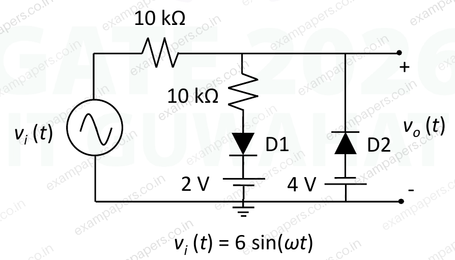
Log in to check the answer
You can attempt this question now. Sign in to view the answer key, explanations and discussion.Log in to check answerQuestion 57
Open questionECMSQ2 marksNeeds review
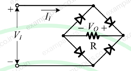
All the diodes in the circuit given below are ideal. Which of the following plots is/are correct when
(in Volts) is swept from
to
? 
Your answerSelect all correct options. You can choose more than one.
Log in to check the answer
You can attempt this question now. Sign in to view the answer key, explanations and discussion.Log in to check answerQuestion 61
Open questionECNAT2 marksNeeds review
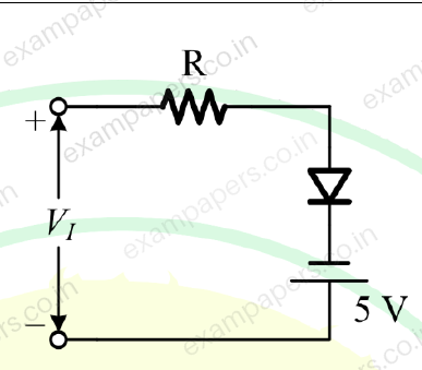
The diode in the circuit shown below is ideal. The input voltage (in Volts) is given by
, where time
is in seconds.The time duration (in ms, rounded off to two decimal places) for which the diode is forward biased during one period of the input is __________.
Log in to check the answer
You can attempt this question now. Sign in to view the answer key, explanations and discussion.Log in to check answerQuestion 23
Open questionECMCQ1 markNeeds review
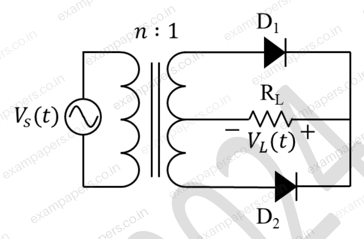
In the circuit shown, the
step-down transformer and the diodes are ideal. The diodes have no voltage drop in forward biased condition. If the input voltage (in Volts) is
and the average value of load voltage
(in Volts) is
, the value of
is ______.
Your answerChoose one option.
Log in to check the answer
You can attempt this question now. Sign in to view the answer key, explanations and discussion.Log in to check answerQuestion 35
Open questionECNAT1 markNeeds review
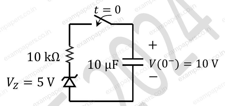
As shown in the circuit given below, the initial voltage across the capacitor is 10 V, with the switch being open. The switch is then closed at
. The total energy dissipated in the ideal Zener diode (
V) after the switch is closed (in mJ, rounded off to three decimal places) is ________.
Log in to check the answer
You can attempt this question now. Sign in to view the answer key, explanations and discussion.Log in to check answerQuestion 40
Open questionECMCQ2 marksNeeds review
In the circuit shown below, D₁ and D₂ are silicon diodes with cut-in voltage of 0.7 V.
and
are input and output voltages in volts. The transfer characteristic is 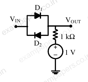
Your answerChoose one option.
Log in to check the answer
You can attempt this question now. Sign in to view the answer key, explanations and discussion.Log in to check answerQuestion 57
Open questionECNAT2 marksNeeds review
A circuit and the characteristics of the diode (D) in it are shown. The ratio of the minimum to the maximum small signal voltage gain
is ________ (rounded off to two decimal places). 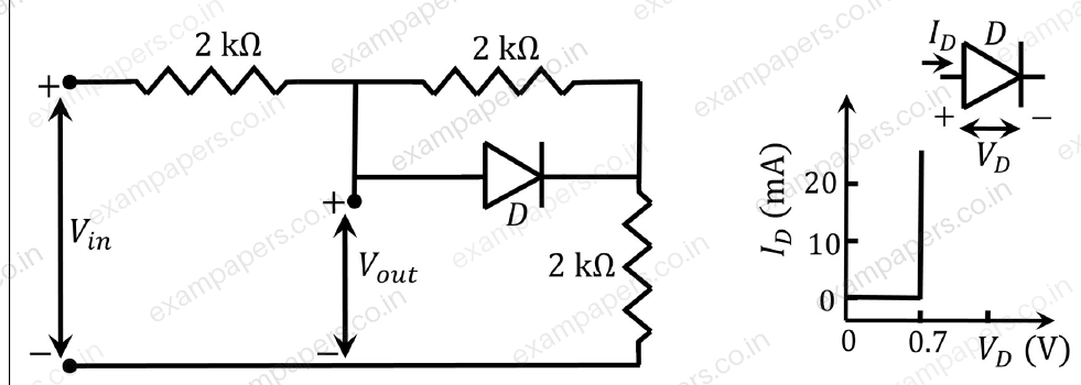
Log in to check the answer
You can attempt this question now. Sign in to view the answer key, explanations and discussion.Log in to check answerQuestion 43
Open questionECNAT2 marksNeeds review
An asymmetrical period pulse train
of 10 V amplitude with on-time
and off-time
is applied to the circuit shown in the figure. The diode
is ideal.The difference between the maximum voltage and minimum voltage of the output waveform
(in integer) is ________ V. 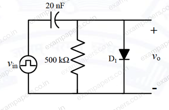
Log in to check the answer
You can attempt this question now. Sign in to view the answer key, explanations and discussion.Log in to check answerQuestion 17
Open questionECNAT1 markNeeds review
In the circuit shown below, all the components are ideal and the input voltage is sinusoidal. The magnitude of the steady-state output
(rounded off to two decimal places) is ______ V. 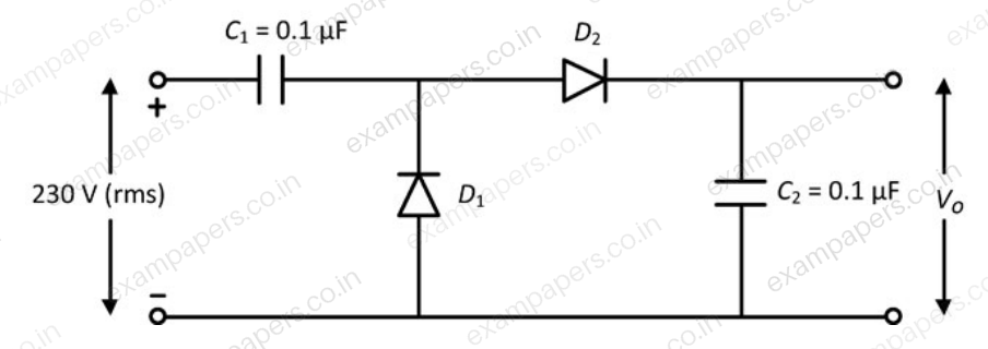
Log in to check the answer
You can attempt this question now. Sign in to view the answer key, explanations and discussion.Log in to check answerQuestion 24
Open questionECNAT1 markNeeds review
In the circuit shown,
is a square wave of period
with maximum and minimum values of 8 V and -10 V, respectively. Assume that the diode is ideal and
. The average value of
is ____ volts (rounded off to 1 decimal place). 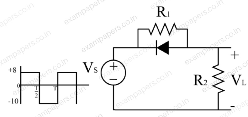
Log in to check the answer
You can attempt this question now. Sign in to view the answer key, explanations and discussion.Log in to check answer