
Electronics and Communication Engineering
GATE ECE format:mcq PYQs
Build your understanding with focused practice from past exam papers.
Questions 261–270 of 426. Imported answers require independent review unless marked reviewed.
Question 29
Open questionECMCQ2 marksNeeds review
A finite duration discrete-time signal
is obtained by sampling the continuous-time signal
at sampling instants
,
. The 8-point discrete Fourier transform (DFT) of
is defined as
Which one of the following statements is TRUE?Your answerChoose one option.
Log in to check the answer
You can attempt this question now. Sign in to view the answer key, explanations and discussion.Log in to check answerQuestion 30
Open questionECMCQ2 marksNeeds review
For the given circuit, which one of the following is the correct state equation?
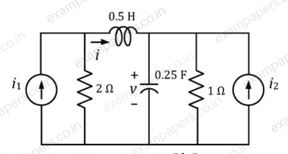
Your answerChoose one option.
Log in to check the answer
You can attempt this question now. Sign in to view the answer key, explanations and discussion.Log in to check answerQuestion 31
Open questionECMCQ2 marksNeeds review
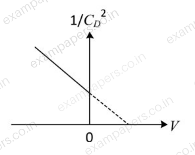
A one-sided abrupt
junction diode has a depletion capacitance
of 50 pF at a reverse bias of 0.2 V. The plot of
versus the applied voltage
for this diode is a straight line as shown in the figure below. The slope of the plot is ______
. 
Your answerChoose one option.
Log in to check the answer
You can attempt this question now. Sign in to view the answer key, explanations and discussion.Log in to check answerQuestion 32
Open questionECMCQ2 marksNeeds review
The band diagram of a
-type semiconductor with a band-gap of 1 eV is shown. Using this semiconductor, a MOS capacitor having
of
V,
of
nF/cm
and a metal work function of 3.87 eV is fabricated. There is no charge in the oxide. If the voltage across the capacitor is
, the magnitude of depletion charge per unit area (in C/cm
) is
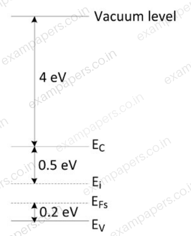
Your answerChoose one option.
Log in to check the answer
You can attempt this question now. Sign in to view the answer key, explanations and discussion.Log in to check answerQuestion 33
Open questionECMCQ2 marksNeeds review
The base of an
BJT T1 has a linear doping profile
as shown below. The base of another
BJT T2 has a uniform doping
of
cm
. All other parameters are identical for both the devices. Assuming that the hole density profile is the same as that of doping, the common-emitter current gain of T2 is
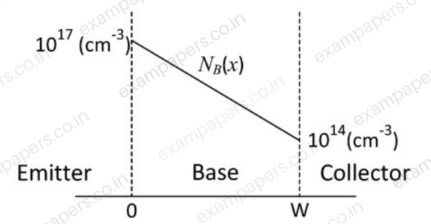
Your answerChoose one option.
Log in to check the answer
You can attempt this question now. Sign in to view the answer key, explanations and discussion.Log in to check answerQuestion 34
Open questionECMCQ2 marksNeeds review
A
junction solar cell of area 1.0 cm
, illuminated uniformly with 100 mW cm
, has the following parameters: Efficiency = 15%, open circuit voltage = 0.7 V, fill factor = 0.8, and thickness = 200 μm. The charge of an electron is
C. The average optical generation rate (in cm
s
) isYour answerChoose one option.
Log in to check the answer
You can attempt this question now. Sign in to view the answer key, explanations and discussion.Log in to check answerQuestion 35
Open questionECMCQ2 marksNeeds review
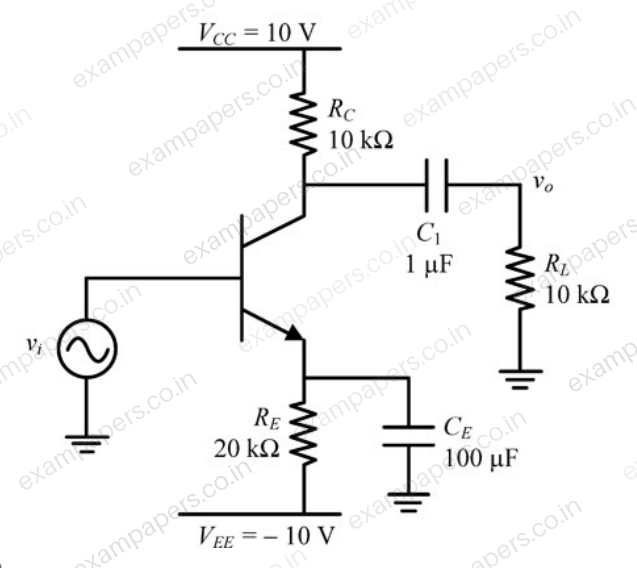
For the BJT in the amplifier shown below,
V,
mV. Assume that BJT output resistance (
) is very high and the base current is negligible. The capacitors are also assumed to be short circuited at signal frequencies. The input
is direct coupled. The low frequency voltage gain
of the amplifier is
Your answerChoose one option.
Log in to check the answer
You can attempt this question now. Sign in to view the answer key, explanations and discussion.Log in to check answerQuestion 36
Open questionECMCQ2 marksNeeds review
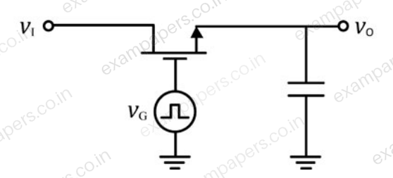
An enhancement MOSFET of threshold voltage 3 V is being used in the sample and hold circuit given below. Assume that the substrate of the MOS device is connected to
V. If the input voltage
lies between
V, the minimum and the maximum values of
required for proper sampling and holding respectively, are
Your answerChoose one option.
Log in to check the answer
You can attempt this question now. Sign in to view the answer key, explanations and discussion.Log in to check answerQuestion 37
Open questionECMCQ2 marksNeeds review
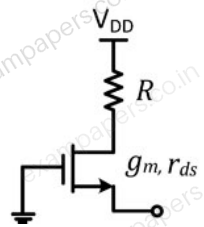
Using the incremental low frequency small-signal model of the MOS device, the Norton equivalent resistance of the following circuit is
Your answerChoose one option.
Log in to check the answer
You can attempt this question now. Sign in to view the answer key, explanations and discussion.Log in to check answerQuestion 38
Open questionECMCQ2 marksNeeds review
P, Q, and R are the decimal integers corresponding to the 4-bit binary number 1100 considered in signed magnitude, 1’s complement, and 2’s complement representations, respectively. The 6-bit 2’s complement representation of (P + Q + R) is
Your answerChoose one option.
Log in to check the answer
You can attempt this question now. Sign in to view the answer key, explanations and discussion.Log in to check answer