
Electronics and Communication Engineering
GATE ECE P-N junction PYQs
Build your understanding with focused practice from past exam papers.
How to practice P-N junction
Attempt a question, record the concept and assumptions, then check the available answer. Rework mistakes after revising the relevant concepts. Topic tags can overlap; review the question context.
Questions 1–10 of 20. Imported answers require independent review unless marked reviewed.
Question 31
Open questionECMSQ1 markNeeds review
Which of the following can be used as an n-type dopant for silicon? Select the correct option(s).
Your answerSelect all correct options. You can choose more than one.
Log in to check the answer
You can attempt this question now. Sign in to view the answer key, explanations and discussion.Log in to check answerQuestion 47
Open questionECMCQ2 marksNeeds review
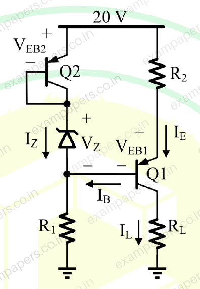
In the circuit shown, the identical transistors Q1 and Q2 are biased in the active region with β = 120. The Zener diode is in the breakdown region with VZ = 5 V and IZ = 25 mA.
If IL = 12 mA and VEB1 = VEB2 = 0.7 V, then the values of R1 and R2 (in kΩ, rounded off to one decimal place) are ______, respectively.
Your answerChoose one option.
Log in to check the answer
You can attempt this question now. Sign in to view the answer key, explanations and discussion.Log in to check answerQuestion 63
Open questionECNAT2 marksNeeds review
An ideal p-n junction germanium diode has a reverse saturation current of 10
A at 300 K.The voltage (in Volts, rounded off to two decimal places) to be applied across the junction to get a forward bias current of 100 mA at 300 K is ____.
(Consider the Boltzman constant
J/K and the charge of an electron
C.)Log in to check the answer
You can attempt this question now. Sign in to view the answer key, explanations and discussion.Log in to check answerQuestion 52
Open questionECMSQ2 marksNeeds review
Which of the following statements is/are true for a BJT with respect to its DC current gain
?Your answerSelect all correct options. You can choose more than one.
Log in to check the answer
You can attempt this question now. Sign in to view the answer key, explanations and discussion.Log in to check answerQuestion 61
Open questionECNAT2 marksNeeds review
Consider a MOS capacitor made with p-type silicon. It has an oxide thickness of 100 nm, a fixed positive oxide charge of
at the oxide-silicon interface, and a metal work function of 4.6 eV. Assume that the relative permittivity of the oxide is 4 and the absolute permittivity of free space is
. If the flatband voltage is 0 V, the work function of the p-type silicon (in eV, rounded off to two decimal places) is ______.Log in to check the answer
You can attempt this question now. Sign in to view the answer key, explanations and discussion.Log in to check answerQuestion 64
Open questionECNAT2 marksNeeds review
An NMOS transistor operating in the linear region has
of 5
A at
of 0.1 V. Keeping
constant, the
is increased to 1.5 V.Given that
, the transconductance at the new operating point (in
A/V, rounded off to two decimal places) is ______.Log in to check the answer
You can attempt this question now. Sign in to view the answer key, explanations and discussion.Log in to check answerQuestion 65
Open questionECNAT2 marksNeeds review
The photocurrent of a PN junction diode solar cell is 1 mA. The voltage corresponding to its maximum power point is 0.3 V. If the thermal voltage is 30 mV, the reverse saturation current of the diode (in nA, rounded off to two decimal places) is ______.
Log in to check the answer
You can attempt this question now. Sign in to view the answer key, explanations and discussion.Log in to check answerQuestion 9
Open questionECMCQ1 markNeeds review
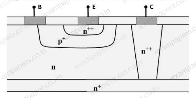
The correct circuit representation of the structure shown in the figure is
Your answerChoose one option.
Log in to check the answer
You can attempt this question now. Sign in to view the answer key, explanations and discussion.Log in to check answerQuestion 10
Open questionECMCQ1 markNeeds review
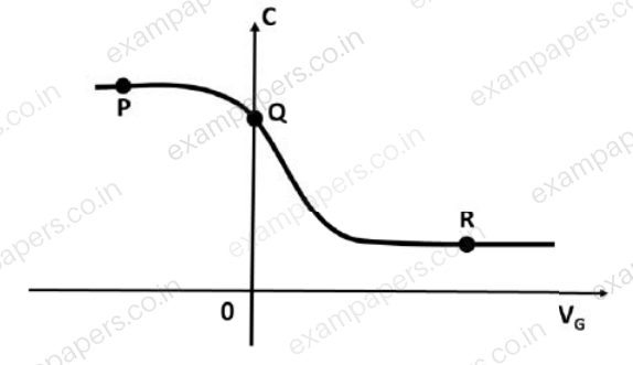
The figure shows the high-frequency C-V curve of a MOS capacitor (at T = 300 K) with
and no oxide charges. The flat-band, inversion, and accumulation conditions are represented, respectively, by the points
Your answerChoose one option.
Log in to check the answer
You can attempt this question now. Sign in to view the answer key, explanations and discussion.Log in to check answerQuestion 35
Open questionECMCQ2 marksNeeds review
The quantum efficiency (
) and responsivity (
) at a wavelength
(in
) in a p-i-n photodetector are related byYour answerChoose one option.
Log in to check the answer
You can attempt this question now. Sign in to view the answer key, explanations and discussion.Log in to check answer