
Electronics and Communication Engineering
GATE ECE Semiconductor devices PYQs
Build your understanding with focused practice from past exam papers.
How to practice Semiconductor devices
Attempt a question, record the concept and assumptions, then check the available answer. Rework mistakes after revising the relevant concepts. Topic tags can overlap; review the question context.
Questions 1–5 of 5. Imported answers require independent review unless marked reviewed.
Question 18
Open questionECMCQ1 markNeeds review
Consider the CMOS circuit shown in the figure (substrates are connected to their respective sources). The gate width (
) to gate length (
) ratios (
) of the transistors are as shown. Both the transistors have the same gate oxide capacitance per unit area. For the
MOSFET, the threshold voltage is
and the mobility of holes is
. For the
MOSFET, the threshold voltage is
and the mobility of electrons is
. The steady state output voltage
is _________. 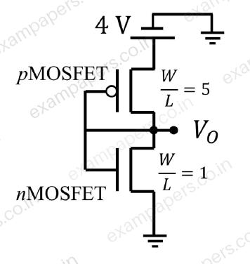
Your answerChoose one option.
Log in to check the answer
You can attempt this question now. Sign in to view the answer key, explanations and discussion.Log in to check answerQuestion 20
Open questionECMCQ1 markNeeds review
The ideal long channel
MOSFET and
MOSFET devices shown in the circuits have threshold voltages of 1 V and
V, respectively. The MOSFET substrates are connected to their respective sources. Ignore leakage currents and assume that the capacitors are initially discharged. For the applied voltages as shown, the steady state voltages are ________________. 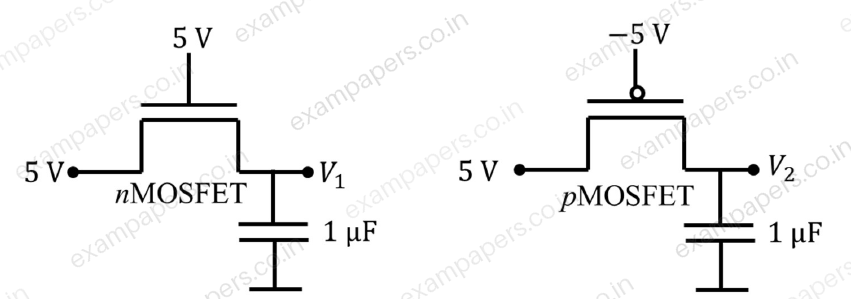
Your answerChoose one option.
Log in to check the answer
You can attempt this question now. Sign in to view the answer key, explanations and discussion.Log in to check answerQuestion 34
Open questionECNAT1 markNeeds review
An ideal MOS capacitor (
-type semiconductor) is shown in the figure. The MOS capacitor is under strong inversion with
V. The corresponding inversion charge density (
) is 2.2
C/cm
. Assume oxide capacitance per unit area as
F/cm
. For
V, the value of
is _____
C/cm
(rounded off to one decimal place). 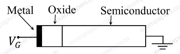
Log in to check the answer
You can attempt this question now. Sign in to view the answer key, explanations and discussion.Log in to check answerQuestion 40
Open questionECMCQ2 marksNeeds review
Consider an ideal long channel nMOSFET (enhancement-mode) with gate length 10 μm and width 100 μm. The product of electron mobility (
) and oxide capacitance per unit area (
) is
mA/V
. The threshold voltage of the transistor is 1 V. For a gate-to-source voltage
V and drain-to-source voltage
V (substrate connected to the source), the maximum value of the drain-to-source current is ______.Your answerChoose one option.
Log in to check the answer
You can attempt this question now. Sign in to view the answer key, explanations and discussion.Log in to check answerQuestion 47
Open questionECMSQ2 marksNeeds review
Select the CORRECT statement(s) regarding semiconductor devices.
Your answerSelect all correct options. You can choose more than one.
Log in to check the answer
You can attempt this question now. Sign in to view the answer key, explanations and discussion.Log in to check answer