
Electronics and Communication Engineering
GATE ECE topic:combinational-circuits PYQs
Build your understanding with focused practice from past exam papers.
Questions 11–19 of 19. Imported answers require independent review unless marked reviewed.
Question 53
Open questionECNAT2 marksNeeds review
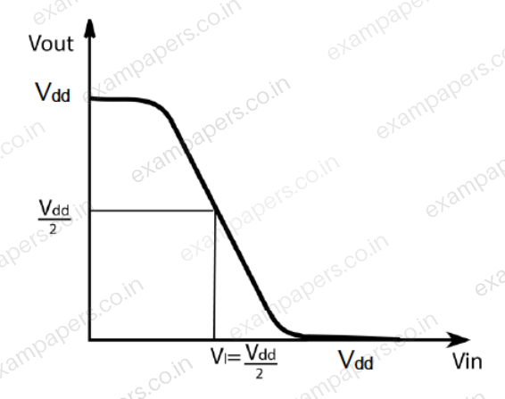
A CMOS inverter, designed to have a mid-point voltage
equal to half of
, as shown in the figure, has the following parameters:
for nMOS
for pMOSThe ratio of
to
is equal to ____ (rounded off to 3 decimal places).
Log in to check the answer
You can attempt this question now. Sign in to view the answer key, explanations and discussion.Log in to check answerQuestion 8
Open questionECMCQ1 markNeeds review
The logic function
realized by the given circuit is 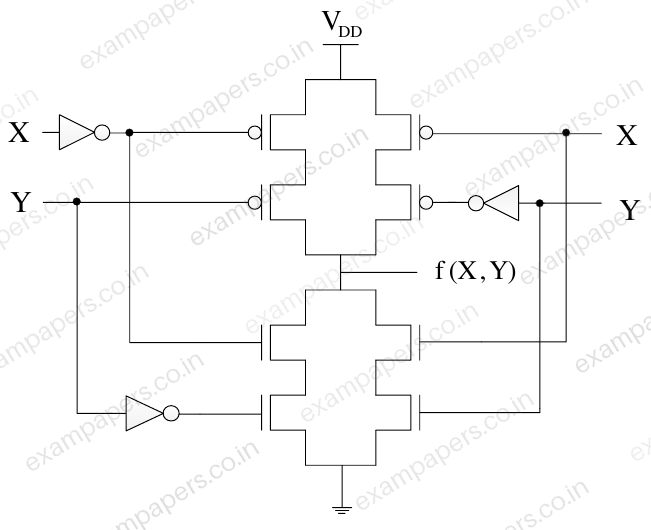
Your answerChoose one option.
Log in to check the answer
You can attempt this question now. Sign in to view the answer key, explanations and discussion.Log in to check answerQuestion 9
Open questionECMCQ1 markNeeds review
A function
defined by three Boolean variables A, B and C when expressed as sum of products is given by
, where,
,
, and
are the complements of the respective variables. The product of sums (POS) form of the function F isYour answerChoose one option.
Log in to check the answer
You can attempt this question now. Sign in to view the answer key, explanations and discussion.Log in to check answerQuestion 31
Open questionECMCQ2 marksNeeds review
A four-variable Boolean function is realized using 4×1 multiplexers as shown in the figure.
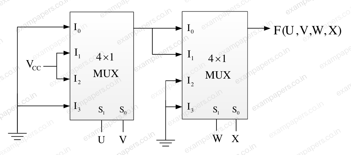
The minimized expression for F(U,V,W,X) is
Your answerChoose one option.
Log in to check the answer
You can attempt this question now. Sign in to view the answer key, explanations and discussion.Log in to check answerQuestion 47
Open questionECNAT2 marksNeeds review
The logic gates shown in the digital circuit below use strong pull-down nMOS transistors for LOW logic level at the outputs. When the pull-downs are off, high-value resistors set the output logic levels to HIGH (i.e. the pull-ups are weak). Note that some nodes are intentionally shorted to implement “wired logic”. Such shorted nodes will be HIGH only if the outputs of all the gates whose outputs are shorted are HIGH.
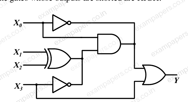
The number of distinct values of
(out of the 16 possible values) that give
is ______.Log in to check the answer
You can attempt this question now. Sign in to view the answer key, explanations and discussion.Log in to check answerQuestion 15
Open questionECMCQ1 markNeeds review
For the circuit shown in the figure,
and
are the inputs and
is the output. 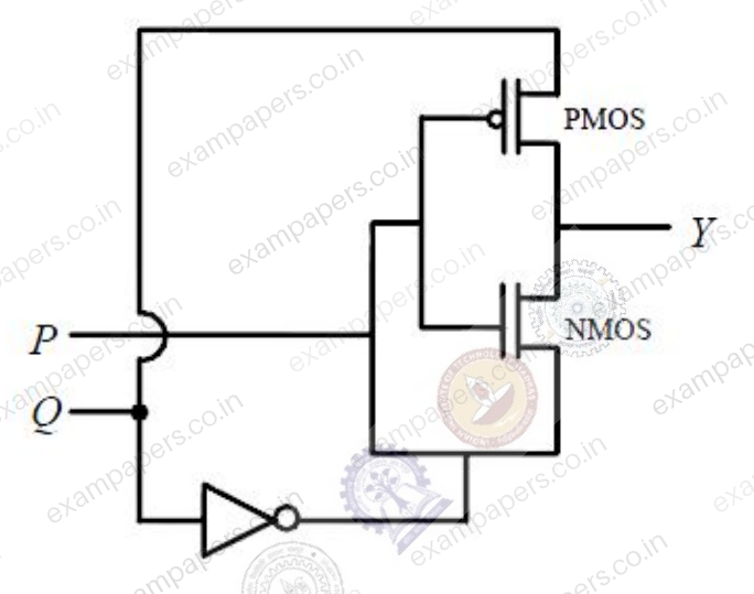
The logic implemented by the circuit is
Your answerChoose one option.
Log in to check the answer
You can attempt this question now. Sign in to view the answer key, explanations and discussion.Log in to check answerQuestion 16
Open questionECMCQ1 markNeeds review
Consider the circuit shown in the figure.
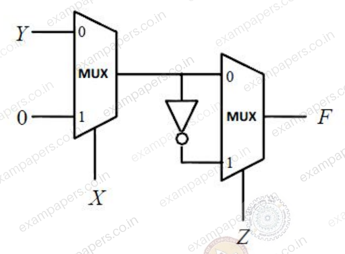
The Boolean expression
implemented by the circuit isYour answerChoose one option.
Log in to check the answer
You can attempt this question now. Sign in to view the answer key, explanations and discussion.Log in to check answerQuestion 44
Open questionECNAT2 marksNeeds review
Figure I shows a 4-bit ripple carry adder realized using full adders and Figure II shows the circuit of a full-adder (FA). The propagation delay of the XOR, AND and OR gates in Figure II are 20 ns, 15 ns and 10 ns, respectively. Assume all the inputs to the 4-bit adder are initially reset to 0.
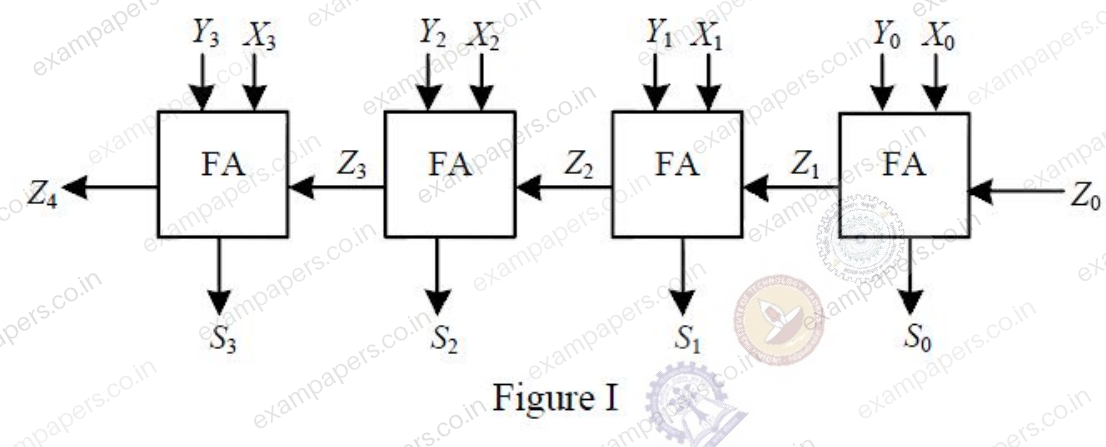
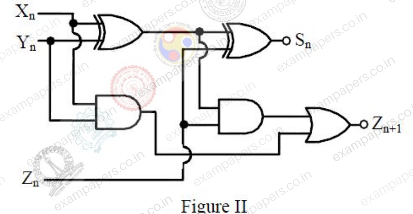
At
, the inputs to the 4-bit adder are changed to
,
and
. The output of the ripple carry adder will be stable at
(in ns) = ______Log in to check the answer
You can attempt this question now. Sign in to view the answer key, explanations and discussion.Log in to check answerQuestion 45
Open questionECMCQ2 marksNeeds review
A programmable logic array (PLA) is shown in the figure. The Boolean function
implemented is 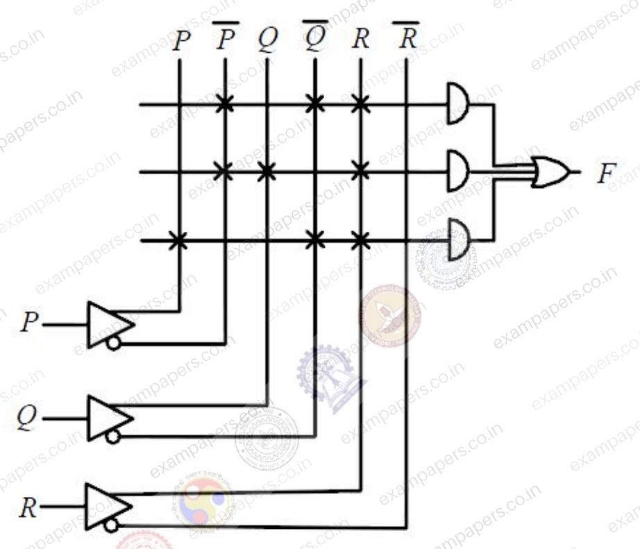
Your answerChoose one option.
Log in to check the answer
You can attempt this question now. Sign in to view the answer key, explanations and discussion.Log in to check answer