
GATE ECE · 2017 · EC
Question 44: Combinational circuits
Give it a try, then reveal the answer to check your work.
Question 44
ECNAT2 marksNeeds review
Figure I shows a 4-bit ripple carry adder realized using full adders and Figure II shows the circuit of a full-adder (FA). The propagation delay of the XOR, AND and OR gates in Figure II are 20 ns, 15 ns and 10 ns, respectively. Assume all the inputs to the 4-bit adder are initially reset to 0.
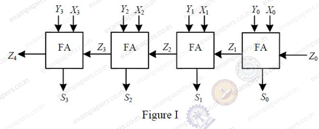
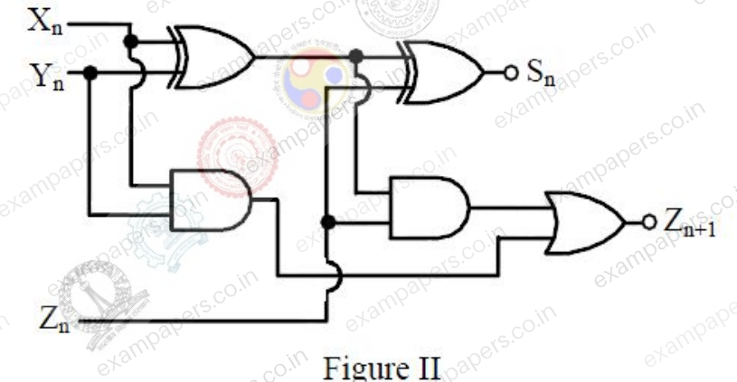
At
, the inputs to the 4-bit adder are changed to
,
and
. The output of the ripple carry adder will be stable at
(in ns) = ______Log in to check the answer
You can attempt this question now. Sign in to view the answer key, explanations and discussion.Log in to check answerEXPLORE & PRACTISE
Paper and topic context
See where this question comes from and choose what to practise next.
2017EC
GATE ECE 2017 · Paper 2
Electronics and Communication Engineering · Original paper archive
- Section
- Electronics and Communication Engineering
- Question type
- Numerical answer (NAT)
- Marks
- 2 marks
Practise related topics
Explore more previous year questions using this question’s imported topic tags.
electronics
GATE ECE previous year questions
communication engineering
GATE ECE previous year questions
signals and systems
GATE ECE previous year questions
combinational circuits
GATE ECE previous year questions
Comments
Ask a question, share your approach, or help someone understand.
Log in to view the discussion
You’re not logged in. Log in or create an account to see discussions and add comments.