
Electronics and Communication Engineering
GATE ECE topic:electronic-devices PYQs
Build your understanding with focused practice from past exam papers.
Questions 11–20 of 20. Imported answers require independent review unless marked reviewed.
Question 30
Open questionECMCQ2 marksNeeds review
For an n-channel silicon MOSFET with 10 nm gate oxide thickness, the substrate sensitivity
is found to be 50 mV/V at a substrate voltage
V, where
is the threshold voltage of the MOSFET. Assume that,
, where
is the separation between the Fermi energy level
and the intrinsic level
in the bulk. Parameters given areElectron charge
C
Vacuum permittivity
F/m
Relative permittivity of silicon
Relative permittivity of oxide
The doping concentration of the substrate is
Your answerChoose one option.
Log in to check the answer
You can attempt this question now. Sign in to view the answer key, explanations and discussion.Log in to check answerQuestion 42
Open questionECNAT2 marksNeeds review
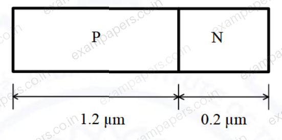
A silicon P-N junction is shown in the figure. The doping in the P region is
and doping in the N region is
. The parameters given areBuilt-in voltage (
) = 0.8 VElectron charge (
) =
CVacuum permittivity (
) =
F/mRelative permittivity of silicon (
) = 12The magnitude of reverse bias voltage that would completely deplete one of the two regions (P or N) prior to the other (rounded off to one decimal place) is ________ V.
Log in to check the answer
You can attempt this question now. Sign in to view the answer key, explanations and discussion.Log in to check answerQuestion 44
Open questionECNAT2 marksNeeds review
For the transistor
in the circuit shown in the figure,
and
, where
is the mobility of electron,
is the oxide capacitance per unit area,
is the width and
is the length. The channel length modulation coefficient is ignored. If the gate-to-source voltage
is 1 V to keep the transistor at the edge of saturation, the threshold voltage of the transistor (rounded off to one decimal place) is ______ V. 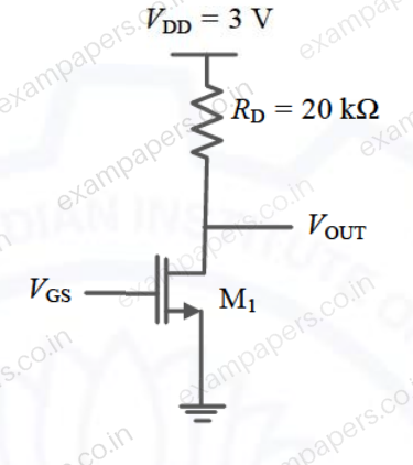
Log in to check the answer
You can attempt this question now. Sign in to view the answer key, explanations and discussion.Log in to check answerQuestion 6
Open questionECMCQ1 markNeeds review
A single crystal intrinsic semiconductor is at a temperature of 300 K with effective density of states for holes twice that of electrons. The thermal voltage is 26 mV.
The intrinsic Fermi level is shifted from mid-band energy level by
Your answerChoose one option.
Log in to check the answer
You can attempt this question now. Sign in to view the answer key, explanations and discussion.Log in to check answerQuestion 7
Open questionECMCQ1 markNeeds review
Consider the recombination process via bulk traps in a forward biased
homojunction diode. The maximum recombination rate is
. If the electron and the hole capture cross-sections are equal, which one of the following is FALSE?Your answerChoose one option.
Log in to check the answer
You can attempt this question now. Sign in to view the answer key, explanations and discussion.Log in to check answerQuestion 31
Open questionECMCQ2 marksNeeds review
A one-sided abrupt
junction diode has a depletion capacitance
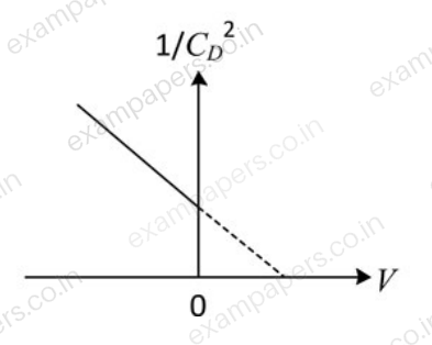
of 50 pF at a reverse bias of 0.2 V. The plot of
versus the applied voltage
for this diode is a straight line as shown in the figure below. The slope of the plot is ______
. 
Your answerChoose one option.
Log in to check the answer
You can attempt this question now. Sign in to view the answer key, explanations and discussion.Log in to check answerQuestion 32
Open questionECMCQ2 marksNeeds review
The band diagram of a
-type semiconductor with a band-gap of 1 eV is shown. Using this semiconductor, a MOS capacitor having
of
V,
of
nF/cm
and a metal work function of 3.87 eV is fabricated. There is no charge in the oxide. If the voltage across the capacitor is
, the magnitude of depletion charge per unit area (in C/cm
) is
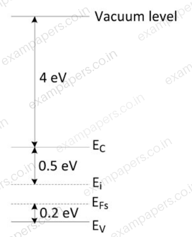
Your answerChoose one option.
Log in to check the answer
You can attempt this question now. Sign in to view the answer key, explanations and discussion.Log in to check answerQuestion 33
Open questionECMCQ2 marksNeeds review
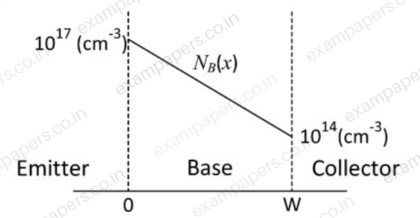
The base of an
BJT T1 has a linear doping profile
as shown below. The base of another
BJT T2 has a uniform doping
of
cm
. All other parameters are identical for both the devices. Assuming that the hole density profile is the same as that of doping, the common-emitter current gain of T2 is
Your answerChoose one option.
Log in to check the answer
You can attempt this question now. Sign in to view the answer key, explanations and discussion.Log in to check answerQuestion 34
Open questionECMCQ2 marksNeeds review
A
junction solar cell of area 1.0 cm
, illuminated uniformly with 100 mW cm
, has the following parameters: Efficiency = 15%, open circuit voltage = 0.7 V, fill factor = 0.8, and thickness = 200 μm. The charge of an electron is
C. The average optical generation rate (in cm
s
) isYour answerChoose one option.
Log in to check the answer
You can attempt this question now. Sign in to view the answer key, explanations and discussion.Log in to check answerQuestion 36
Open questionECMCQ2 marksNeeds review
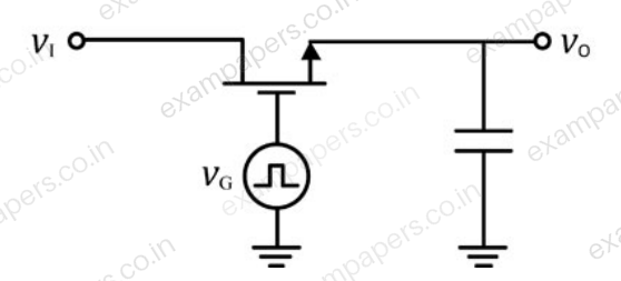
An enhancement MOSFET of threshold voltage 3 V is being used in the sample and hold circuit given below. Assume that the substrate of the MOS device is connected to
V. If the input voltage
lies between
V, the minimum and the maximum values of
required for proper sampling and holding respectively, are
Your answerChoose one option.
Log in to check the answer
You can attempt this question now. Sign in to view the answer key, explanations and discussion.Log in to check answer