
Electrical Engineering
GATE EE Analog and Digital Electronics PYQs
Build your understanding with focused practice from past exam papers.
Questions 31–40 of 57. Imported answers require independent review unless marked reviewed.
Question 52
Open questionEENAT2 marksNeeds review
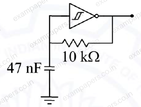
A CMOS Schmitt-trigger inverter has a low output level of 0 V and a high output level of 5 V. It has input thresholds of 1.6 V and 2.4 V. The input capacitance and output resistance of the Schmitt-trigger are negligible. The frequency of the oscillator shown is ________ Hz.
(Round off to 2 decimal places.)
Log in to check the answer
You can attempt this question now. Sign in to view the answer key, explanations and discussion.Log in to check answerQuestion 14
Open questionEEMCQ1 markNeeds review
A common-source amplifier with a drain resistance,
, is powered using a 10 V power supply. Assuming that the transconductance,
, is 520
A/V, the voltage gain of the amplifier is closest to:Your answerChoose one option.
Log in to check the answer
You can attempt this question now. Sign in to view the answer key, explanations and discussion.Log in to check answerQuestion 15
Open questionEEMCQ1 markNeeds review
A sequence detector is designed to detect precisely 3 digital inputs, with overlap sequences detectable. For the sequence (1,0,1) and input data (1,1,0,1,0,0,1,1,0,1,0,1,1,0), what is the output of this detector?
Your answerChoose one option.
Log in to check the answer
You can attempt this question now. Sign in to view the answer key, explanations and discussion.Log in to check answerQuestion 25
Open questionEENAT1 markNeeds review
The cross-section of a metal-oxide-semiconductor structure is shown schematically.

Starting from an uncharged condition, a bias of +3 V is applied to the gate contact with respect to the body contact. The charge inside the silicon dioxide layer is then measured to be +Q. The total charge contained within the dashed box shown, upon application of bias, expressed as a multiple of Q (absolute value in Coulombs, rounded off to the nearest integer) is ________.
Log in to check the answer
You can attempt this question now. Sign in to view the answer key, explanations and discussion.Log in to check answerQuestion 30
Open questionEEMCQ2 marksNeeds review
Consider the diode circuit shown below. The diode D obeys the current-voltage characteristic
, where
,
,
is the voltage across the diode and
is the current through it. The circuit is biased so that voltage,
and current,
. If you had to design this circuit to transfer maximum power from the current source (
) to a resistive load (not shown at the output), what values of
and
would you choose? 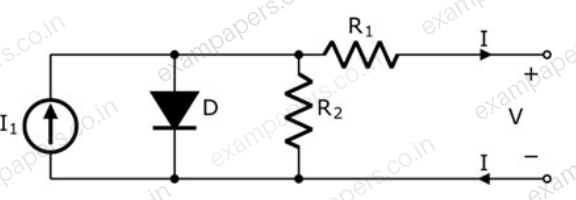
Your answerChoose one option.
Log in to check the answer
You can attempt this question now. Sign in to view the answer key, explanations and discussion.Log in to check answerQuestion 31
Open questionEEMCQ2 marksNeeds review
A non-ideal diode is biased with a voltage of −0.03 V, and a diode current of
is measured. The thermal voltage is 26 mV and the ideality factor for the diode is 15/13. The voltage, in V, at which the measured current increases to
is closest to:Your answerChoose one option.
Log in to check the answer
You can attempt this question now. Sign in to view the answer key, explanations and discussion.Log in to check answerQuestion 54
Open questionEENAT2 marksNeeds review
An 8085 microprocessor accesses two memory locations (2001H) and (2002H), that contain 8-bit numbers 98H and B1H, respectively. The following program is executed:
LXI H,2001H
MVI A, 21H
INX H
ADD M
INX H
MOV M, A
HLT
At the end of this program, the memory location 2003H contains the number in decimal (base 10) form ________.
Log in to check the answer
You can attempt this question now. Sign in to view the answer key, explanations and discussion.Log in to check answerQuestion 16
Open questionEEMCQ1 markNeeds review
Given,
is the gate-source voltage,
is the drain source voltage, and
is the threshold voltage of an enhancement type NMOS transistor, the conditions for transistor to be biased in saturation areYour answerChoose one option.
Log in to check the answer
You can attempt this question now. Sign in to view the answer key, explanations and discussion.Log in to check answerQuestion 33
Open questionEEMCQ2 marksNeeds review
The enhancement type MOSFET in the circuit below operates according to the square law.
, the threshold voltage (
) is 500 mV. Ignore channel length modulation. The output voltage
is 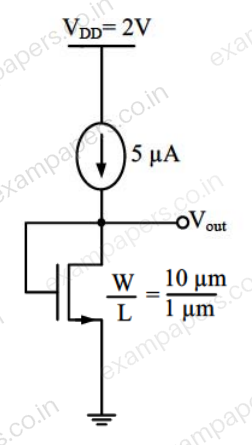
Your answerChoose one option.
Log in to check the answer
You can attempt this question now. Sign in to view the answer key, explanations and discussion.Log in to check answerQuestion 34
Open questionEEMCQ2 marksNeeds review
In the circuit below, the operational amplifier is ideal. If
mV and
mV, the output voltage (
) is 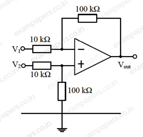
Your answerChoose one option.
Log in to check the answer
You can attempt this question now. Sign in to view the answer key, explanations and discussion.Log in to check answer