
Electronics and Communication Engineering
2017 · Paper 2
Take it one question at a time. Try an answer, then check your understanding.
Complete GATE ECE 2017 Paper 2 overview, original pages and practice · Timed previous-paper practice
Questions 13–15 of 65. Imported answers require review unless explicitly marked reviewed.
Question 13
Open questionECMCQ1 markNeeds review
In the figure, D1 is a real silicon
junction diode with a drop of 0.7 V under forward bias condition and D2 is a Zener diode with breakdown voltage of
V. The input
is a periodic square wave of period T, whose one period is shown in the figure. 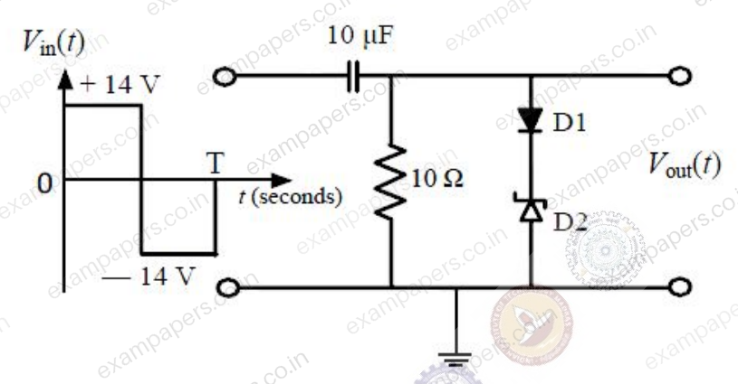
Assuming
, where
is the time constant of the circuit, the maximum and minimum values of the output waveform are respectivelyYour answerChoose one option.
Log in to check the answer
You can attempt this question now. Sign in to view the answer key, explanations and discussion.Log in to check answerQuestion 14
Open questionECNAT1 markNeeds review
Consider the circuit shown in the figure. Assume base-to-emitter voltage
and common-base current gain
of the transistor is unity. 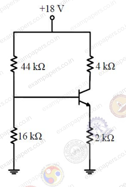
The value of the collector-to-emitter voltage
(in volt) is _____.Log in to check the answer
You can attempt this question now. Sign in to view the answer key, explanations and discussion.Log in to check answerQuestion 15
Open questionECMCQ1 markNeeds review
For the circuit shown in the figure,
and
are the inputs and
is the output. 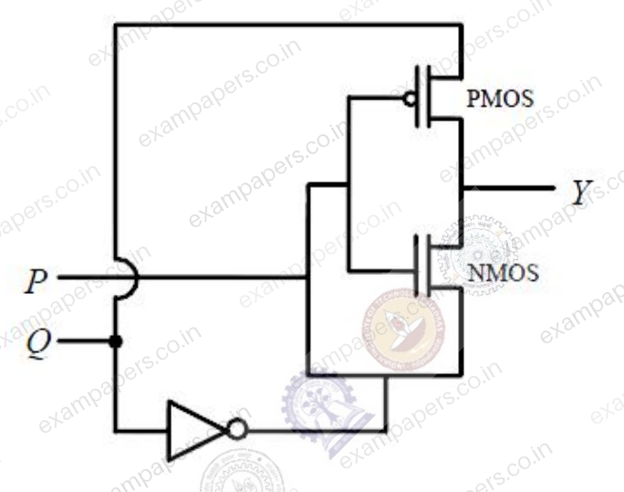
The logic implemented by the circuit is
Your answerChoose one option.
Log in to check the answer
You can attempt this question now. Sign in to view the answer key, explanations and discussion.Log in to check answer