
Electronics and Communication Engineering
GATE ECE format:nat PYQs
Build your understanding with focused practice from past exam papers.
Questions 221–230 of 239. Imported answers require independent review unless marked reviewed.
Question 37
Open questionECNAT2 marksNeeds review
As shown, a uniformly doped Silicon (Si) bar of length
with a donor concentration
is illuminated at
such that electron and hole pairs are generated at the rate of
,
, where
. Hole lifetime is
s, electronic charge
, hole diffusion coefficient
and low level injection condition prevails. Assuming a linearly decaying steady state excess hole concentration that goes to 0 at
, the magnitude of the diffusion current density at
, in A/cm
, is __________.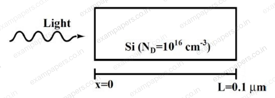
Log in to check the answer
You can attempt this question now. Sign in to view the answer key, explanations and discussion.Log in to check answerQuestion 37
Open questionECNAT2 marksNeeds review
For a particular intensity of incident light on a silicon
junction solar cell, the photocurrent density (
) is 2.5 mA/cm
and the open-circuit voltage (
) is 0.451 V. Consider thermal voltage (
) to be 25 mV. If the intensity of the incident light is increased by 20 times, assuming that the temperature remains unchanged,
(in volts) will be ________.Log in to check the answer
You can attempt this question now. Sign in to view the answer key, explanations and discussion.Log in to check answerQuestion 38
Open questionECNAT2 marksNeeds review
As shown, two Silicon (Si) abrupt
-
junction diodes are fabricated with uniform donor doping concentrations of
and
in the
-regions of the diodes, and uniform acceptor doping concentrations of
and
in the
-regions of the diodes, respectively. Assuming that the reverse bias voltage is
built-in potentials of the diodes, the ratio
of their reverse bias capacitances for the same applied reverse bias, is ________. 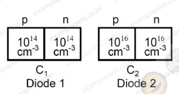
Log in to check the answer
You can attempt this question now. Sign in to view the answer key, explanations and discussion.Log in to check answerQuestion 39
Open questionECNAT2 marksNeeds review
In the figure shown, the
transistor acts as a switch. 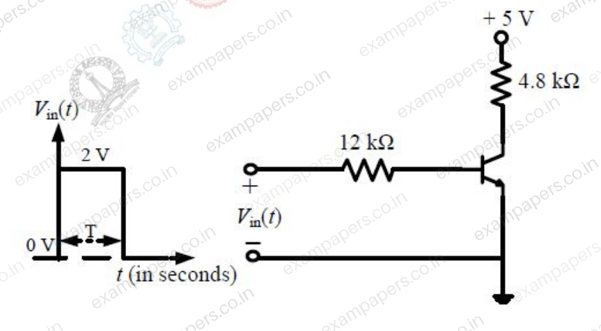
For the input
as shown in the figure, the transistor switches between the cut-off and saturation regions of operation, when T is large. Assume collector-to-emitter voltage at saturation
and base-to-emitter voltage
. The minimum value of the common-base current gain (
) of the transistor for the switching should be ________.Log in to check the answer
You can attempt this question now. Sign in to view the answer key, explanations and discussion.Log in to check answerQuestion 40
Open questionECNAT2 marksNeeds review
For the circuit shown, assume that the NMOS transistor is in saturation. Its threshold voltage
and its transconductance parameter
. Neglect channel length modulation and body bias effects. Under these conditions, the drain current
in mA is ____________. 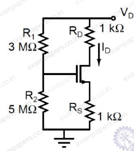
Log in to check the answer
You can attempt this question now. Sign in to view the answer key, explanations and discussion.Log in to check answerQuestion 41
Open questionECNAT2 marksNeeds review
For the DC analysis of the Common-Emitter amplifier shown, neglect the base current and assume that the emitter and collector currents are equal. Given that
,
, and the BJT output resistance
is practically infinite. Under these conditions, the midband voltage gain magnitude,
, is ____________. 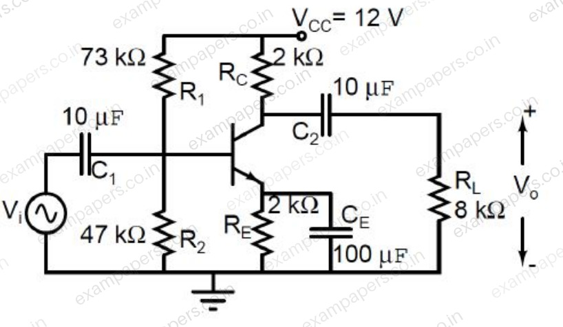
Log in to check the answer
You can attempt this question now. Sign in to view the answer key, explanations and discussion.Log in to check answerQuestion 41
Open questionECNAT2 marksNeeds review
In the circuit shown, transistors Q1 and Q2 are biased at a collector current of 2.6 mA. Assuming that transistor current gains are sufficiently large to assume collector current equal to emitter current and thermal voltage of 26 mV, the magnitude of voltage gain
in the mid-band frequency range is ______ (up to second decimal place). 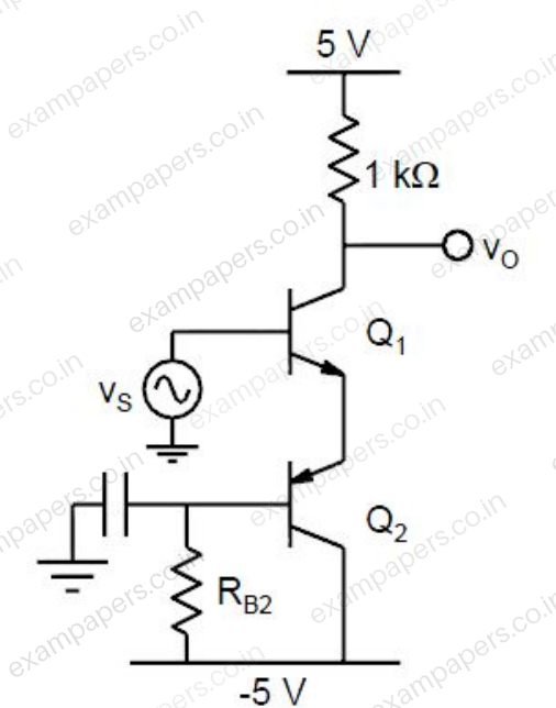
Log in to check the answer
You can attempt this question now. Sign in to view the answer key, explanations and discussion.Log in to check answerQuestion 42
Open questionECNAT2 marksNeeds review
The amplifier circuit shown in the figure is implemented using a compensated operational amplifier (op-amp), and has an open-loop voltage gain,
and an open-loop cut-off frequency,
. The voltage gain of the amplifier at 15 kHz, in V/V, is ____________. 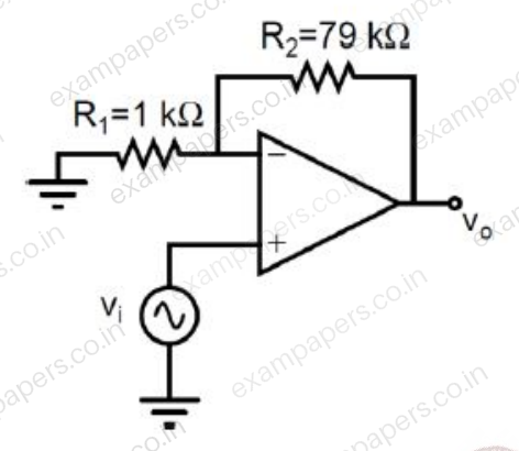
Log in to check the answer
You can attempt this question now. Sign in to view the answer key, explanations and discussion.Log in to check answerQuestion 42
Open questionECNAT2 marksNeeds review
In the voltage reference circuit shown in the figure, the op-amp is ideal and the transistors Q₁, Q₂, ..., Q₃ are identical in all respects and have infinitely large values of common-emitter current gain (β). The collector current (
) of the transistors is related to their base-emitter voltage (
) by the relation
, where
is the saturation current. Assume that the voltage
shown in the figure is 0.7 V and the thermal voltage
. 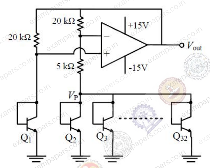
The output voltage
(in volts) is ______Log in to check the answer
You can attempt this question now. Sign in to view the answer key, explanations and discussion.Log in to check answerQuestion 43
Open questionECNAT2 marksNeeds review
The state diagram of a finite state machine (FSM) designed to detect an overlapping sequence of three bits is shown in the figure. The FSM has an input ‘In’ and an output ‘Out’. The initial state of the FSM is S₀.
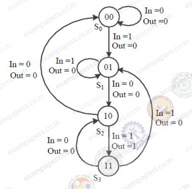
If the input sequence is 10101101001101, starting with the left-most bit, then the number of times ‘Out’ will be 1 is ______
Log in to check the answer
You can attempt this question now. Sign in to view the answer key, explanations and discussion.Log in to check answer