
Electronics and Communication Engineering
GATE ECE Sequential circuits PYQs
Build your understanding with focused practice from past exam papers.
How to practice Sequential circuits
Attempt a question, record the concept and assumptions, then check the available answer. Rework mistakes after revising the relevant concepts. Topic tags can overlap; review the question context.
Questions 1–10 of 24. Imported answers require independent review unless marked reviewed.
Question 27
Open questionECMSQ1 markNeeds review
A binary ripple counter is designed to count
to
. Which of the following is/are the number of flip-flops required to design the counter?Your answerSelect all correct options. You can choose more than one.
Log in to check the answer
You can attempt this question now. Sign in to view the answer key, explanations and discussion.Log in to check answerQuestion 35
Open questionECNAT1 markNeeds review
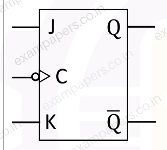
The negative edge triggered JK flip-flop in the Figure has J and K inputs tied to Logic High and a square wave of 10 cycles/second is applied to its clock (C) input. The frequency of the output Q (in cycles/second) is __. (rounded off to two decimal places)
Log in to check the answer
You can attempt this question now. Sign in to view the answer key, explanations and discussion.Log in to check answerQuestion 49
Open questionECMCQ2 marksNeeds review
A shift-left Shift Register (SR) and a D flip-flop are connected to a synchronized clock as shown in the Figure. Assume that the SR and D flip-flops are initially cleared and the XOR gate has no propagation delay.
Which of the following options gives the correct binary representation (
) of the content of the shift register immediately after the 5th clock transition (positive edge)? 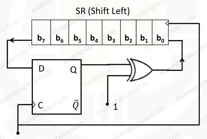
Your answerChoose one option.
Log in to check the answer
You can attempt this question now. Sign in to view the answer key, explanations and discussion.Log in to check answerQuestion 45
Open questionECMCQ2 marksNeeds review
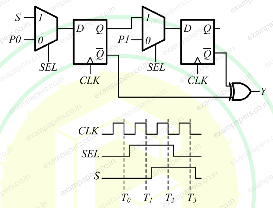
A positive-edge-triggered sequential circuit is shown below. There are no timing violations in the circuit. Input P0 is set to logic ‘0’ and P1 is set to logic ‘1’ at all times. The timing diagram of the inputs SEL and S are also shown below.
The sequence of output Y from time T₀ to T₃ is ________.
Your answerChoose one option.
Log in to check the answer
You can attempt this question now. Sign in to view the answer key, explanations and discussion.Log in to check answerQuestion 62
Open questionECNAT2 marksNeeds review
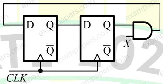
In the circuit shown below, the AND gate has a propagation delay of 1 ns. The edge-triggered flip-flops have a set-up time of 2 ns, a hold-time of 0 ns, and a clock-to-Q delay of 2 ns.
The maximum clock frequency (in MHz, rounded off to the nearest integer) such that there are no setup violations is __________.
Log in to check the answer
You can attempt this question now. Sign in to view the answer key, explanations and discussion.Log in to check answerQuestion 42
Open questionECMCQ2 marksNeeds review
The sequence of states
of the given synchronous sequential circuit is ______.
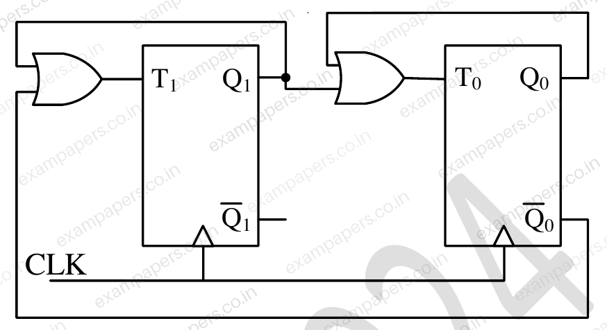
Your answerChoose one option.
Log in to check the answer
You can attempt this question now. Sign in to view the answer key, explanations and discussion.Log in to check answerQuestion 24
Open questionECMCQ1 markNeeds review
The synchronous sequential circuit shown below works at a clock frequency of 1 GHz. The throughput, in Mbits/s, and the latency, in ns, respectively, are
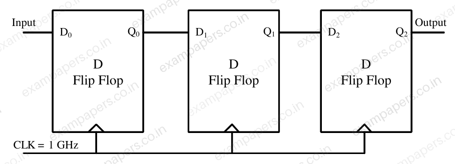
Your answerChoose one option.
Log in to check the answer
You can attempt this question now. Sign in to view the answer key, explanations and discussion.Log in to check answerQuestion 34
Open questionECNAT1 markNeeds review
For the circuit shown below, the propagation delay of each NAND gate is 1 ns. The critical path delay, in ns, is ______ (rounded off to the nearest integer).
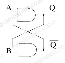
Log in to check the answer
You can attempt this question now. Sign in to view the answer key, explanations and discussion.Log in to check answerQuestion 63
Open questionECNAT2 marksNeeds review
In a given sequential circuit, initial states are
and
. For a clock frequency of 1 MHz, the frequency of signal
in kHz, is _________ (rounded off to the nearest integer).
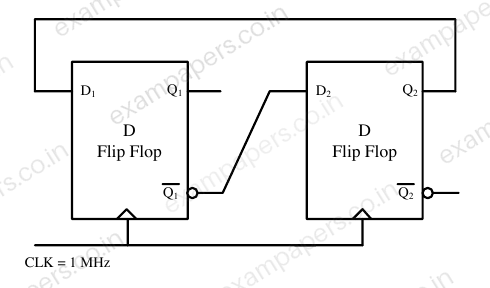
Log in to check the answer
You can attempt this question now. Sign in to view the answer key, explanations and discussion.Log in to check answerQuestion 43
Open questionECMCQ2 marksNeeds review
For the circuit shown, the clock frequency is
and the duty cycle is 25%. For the signal at the Q output of the Flip-Flop, __________. 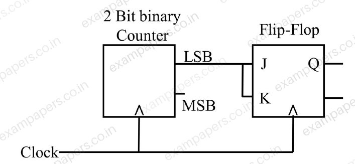
Your answerChoose one option.
Log in to check the answer
You can attempt this question now. Sign in to view the answer key, explanations and discussion.Log in to check answer