
Electronics and Communication Engineering
GATE ECE topic:sequential-circuits PYQs
Build your understanding with focused practice from past exam papers.
Questions 11–20 of 24. Imported answers require independent review unless marked reviewed.
Question 31
Open questionECMCQ2 marksNeeds review
The propagation delays of the XOR gate, AND gate and multiplexer (MUX) in the circuit shown in the figure are 4 ns, 2 ns and 1 ns, respectively.
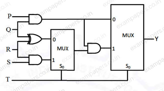
If all the inputs P, Q, R, S and T are applied simultaneously and held constant, the maximum propagation delay of the circuit is
Your answerChoose one option.
Log in to check the answer
You can attempt this question now. Sign in to view the answer key, explanations and discussion.Log in to check answerQuestion 46
Open questionECNAT2 marksNeeds review
The propagation delay of the exclusive-OR (XOR) gate in the circuit in the figure is 3 ns. The propagation delay of all the flip-flops is assumed to be zero. The clock (Clk) frequency provided to the circuit is 500 MHz.
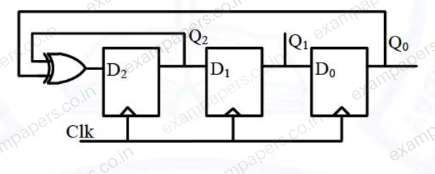
Starting from the initial value of the flip-flop outputs
with
, the minimum number of triggering clock edges after which the flip-flop outputs
becomes 100 (in integer) is ______.Log in to check the answer
You can attempt this question now. Sign in to view the answer key, explanations and discussion.Log in to check answerQuestion 39
Open questionECMCQ2 marksNeeds review
The state diagram of a sequence detector is shown below. State
is the initial state of the sequence detector. If the output is 1, then
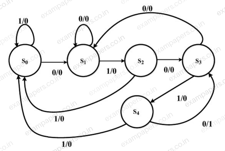
Your answerChoose one option.
Log in to check the answer
You can attempt this question now. Sign in to view the answer key, explanations and discussion.Log in to check answerQuestion 50
Open questionECNAT2 marksNeeds review
For the components in the sequential circuit shown below,
is the propagation delay,
is the setup time, and
is the hold time. The maximum clock frequency (rounded off to the nearest integer), at which the given circuit can operate reliably, is ____ MHz. 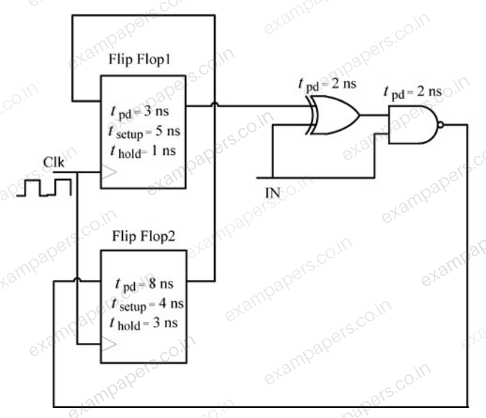
Log in to check the answer
You can attempt this question now. Sign in to view the answer key, explanations and discussion.Log in to check answerQuestion 15
Open questionECMCQ1 markNeeds review
In the circuit shown, A and B are the inputs and F is the output. What is the functionality of the circuit?
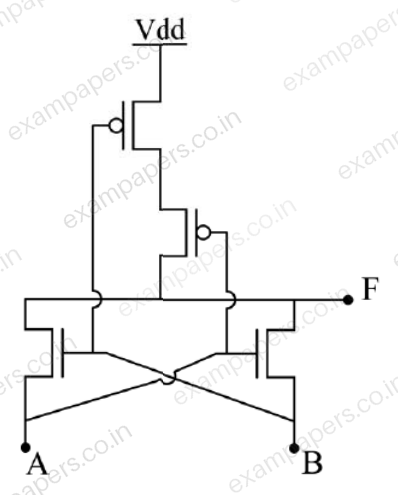
Your answerChoose one option.
Log in to check the answer
You can attempt this question now. Sign in to view the answer key, explanations and discussion.Log in to check answerQuestion 25
Open questionECNAT1 markNeeds review
In the circuit shown, the clock frequency, i.e., the frequency of the Clk signal, is 12 kHz. The frequency of the signal at
is ____ kHz. 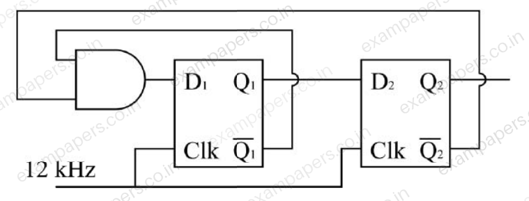
Log in to check the answer
You can attempt this question now. Sign in to view the answer key, explanations and discussion.Log in to check answerQuestion 39
Open questionECMCQ2 marksNeeds review
The state transition diagram for the circuit shown is
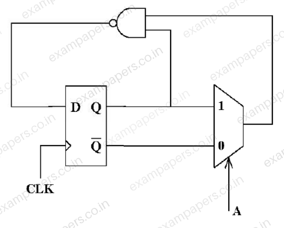
Your answerChoose one option.
Log in to check the answer
You can attempt this question now. Sign in to view the answer key, explanations and discussion.Log in to check answerQuestion 19
Open questionECNAT1 markNeeds review
A traffic signal cycles from GREEN to YELLOW, YELLOW to RED and RED to GREEN. In each cycle, GREEN is turned on for 70 seconds, YELLOW is turned on for 5 seconds and the RED is turned on for 75 seconds. This traffic light has to be implemented using a finite state machine (FSM). The only input to this FSM is a clock of 5 second period. The minimum number of flip-flops required to implement this FSM is ______.
Log in to check the answer
You can attempt this question now. Sign in to view the answer key, explanations and discussion.Log in to check answerQuestion 46
Open questionECNAT2 marksNeeds review
In the circuit shown below, a positive edge-triggered D Flip-Flop is used for sampling input data
using clock
. The XOR gate outputs 3.3 volts for logic HIGH and 0 volts for logic LOW levels. The data bit and clock periods are equal and the value of
, where the parameters
and
are shown in the figure. Assume that the Flip-Flop and the XOR gate are ideal. 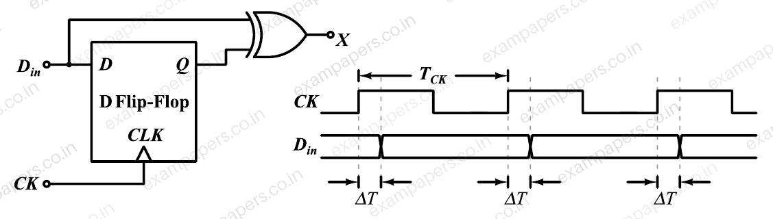
If the probability of input data bit (
) transition in each clock period is 0.3, the average value (in volts, accurate to two decimal places) of the voltage at node
, is ________.Log in to check the answer
You can attempt this question now. Sign in to view the answer key, explanations and discussion.Log in to check answerQuestion 15
Open questionECMCQ1 markNeeds review
In the latch circuit shown, the NAND gates have non-zero, but unequal propagation delays. The present input condition is: P = Q = ‘0’. If the input condition is changed simultaneously to P = Q = ‘1’, the outputs X and Y are
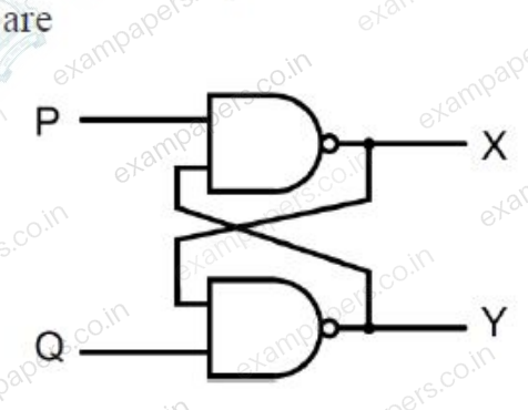
Your answerChoose one option.
Log in to check the answer
You can attempt this question now. Sign in to view the answer key, explanations and discussion.Log in to check answer