
Electronics and Communication Engineering
GATE ECE year:2017 PYQs
Build your understanding with focused practice from past exam papers.
Questions 81–90 of 130. Imported answers require independent review unless marked reviewed.
Question 41
Open questionECNAT2 marksNeeds review
For the DC analysis of the Common-Emitter amplifier shown, neglect the base current and assume that the emitter and collector currents are equal. Given that
,
, and the BJT output resistance
is practically infinite. Under these conditions, the midband voltage gain magnitude,
, is ____________. 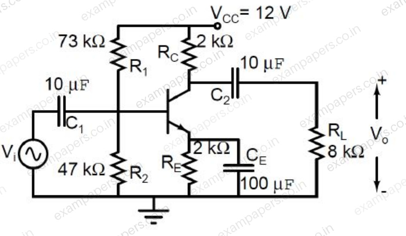
Log in to check the answer
You can attempt this question now. Sign in to view the answer key, explanations and discussion.Log in to check answerQuestion 41
Open questionECNAT2 marksNeeds review
In the circuit shown, transistors Q1 and Q2 are biased at a collector current of 2.6 mA. Assuming that transistor current gains are sufficiently large to assume collector current equal to emitter current and thermal voltage of 26 mV, the magnitude of voltage gain
in the mid-band frequency range is ______ (up to second decimal place). 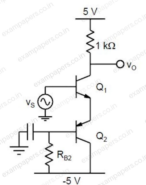
Log in to check the answer
You can attempt this question now. Sign in to view the answer key, explanations and discussion.Log in to check answerQuestion 42
Open questionECNAT2 marksNeeds review
The amplifier circuit shown in the figure is implemented using a compensated operational amplifier (op-amp), and has an open-loop voltage gain,
and an open-loop cut-off frequency,
. The voltage gain of the amplifier at 15 kHz, in V/V, is ____________. 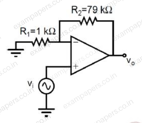
Log in to check the answer
You can attempt this question now. Sign in to view the answer key, explanations and discussion.Log in to check answerQuestion 42
Open questionECNAT2 marksNeeds review
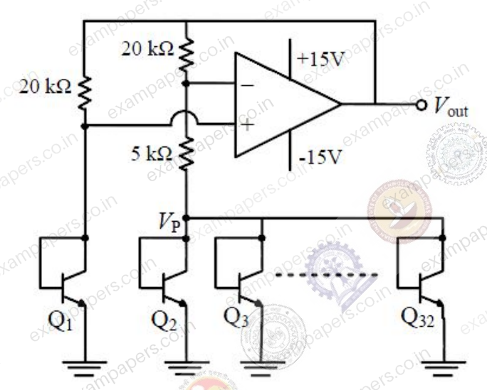
In the voltage reference circuit shown in the figure, the op-amp is ideal and the transistors Q₁, Q₂, ..., Q₃ are identical in all respects and have infinitely large values of common-emitter current gain (β). The collector current (
) of the transistors is related to their base-emitter voltage (
) by the relation
, where
is the saturation current. Assume that the voltage
shown in the figure is 0.7 V and the thermal voltage
. 
The output voltage
(in volts) is ______Log in to check the answer
You can attempt this question now. Sign in to view the answer key, explanations and discussion.Log in to check answerQuestion 43
Open questionECMCQ2 marksNeeds review
Which one of the following gives the simplified sum of products expression for the Boolean function
, where
,
,
and
are minterms corresponding to the inputs
,
and
with
as the MSB and
as the LSB?Your answerChoose one option.
Log in to check the answer
You can attempt this question now. Sign in to view the answer key, explanations and discussion.Log in to check answerQuestion 43
Open questionECNAT2 marksNeeds review
The state diagram of a finite state machine (FSM) designed to detect an overlapping sequence of three bits is shown in the figure. The FSM has an input ‘In’ and an output ‘Out’. The initial state of the FSM is S₀.
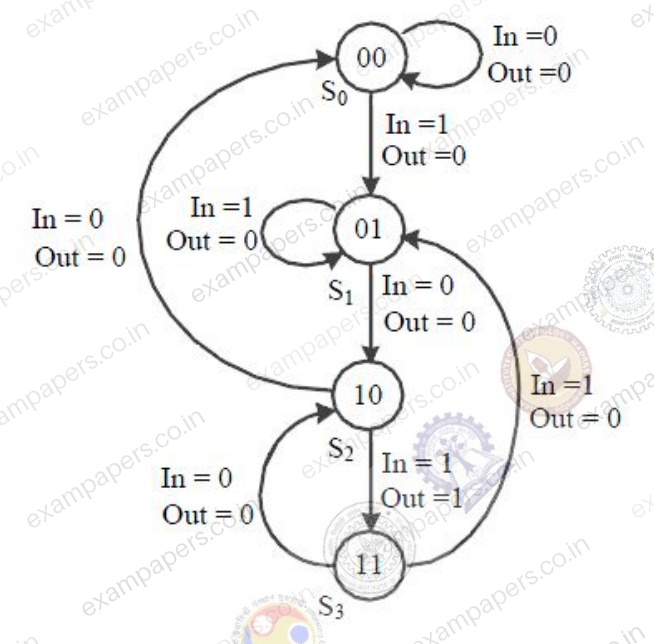
If the input sequence is 10101101001101, starting with the left-most bit, then the number of times ‘Out’ will be 1 is ______
Log in to check the answer
You can attempt this question now. Sign in to view the answer key, explanations and discussion.Log in to check answerQuestion 44
Open questionECNAT2 marksNeeds review
A 4-bit shift register circuit configured for right-shift operation, i.e.
,
,
,
, is shown. If the present state of the shift register is
, the number of clock cycles required to reach the state
is ____________. 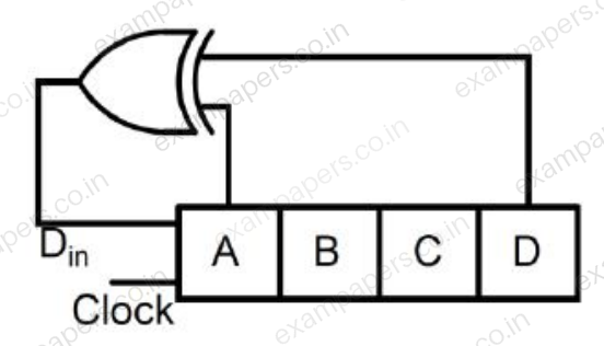
Log in to check the answer
You can attempt this question now. Sign in to view the answer key, explanations and discussion.Log in to check answerQuestion 44
Open questionECNAT2 marksNeeds review
Figure I shows a 4-bit ripple carry adder realized using full adders and Figure II shows the circuit of a full-adder (FA). The propagation delay of the XOR, AND and OR gates in Figure II are 20 ns, 15 ns and 10 ns, respectively. Assume all the inputs to the 4-bit adder are initially reset to 0.
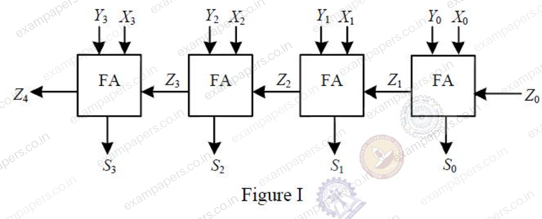
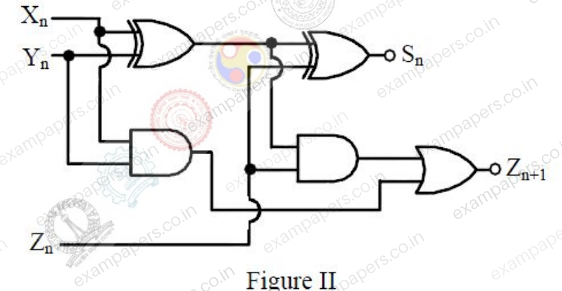
At
, the inputs to the 4-bit adder are changed to
,
and
. The output of the ripple carry adder will be stable at
(in ns) = ______Log in to check the answer
You can attempt this question now. Sign in to view the answer key, explanations and discussion.Log in to check answerQuestion 45
Open questionECMCQ2 marksNeeds review
The following FIVE instructions were executed on an 8085 microprocessor.
MVI A, 33H
MVI B, 78H
ADD B
CMA
ANI 32H
The Accumulator value immediately after the execution of the fifth instruction is
Your answerChoose one option.
Log in to check the answer
You can attempt this question now. Sign in to view the answer key, explanations and discussion.Log in to check answerQuestion 45
Open questionECMCQ2 marksNeeds review
A programmable logic array (PLA) is shown in the figure. The Boolean function
implemented is 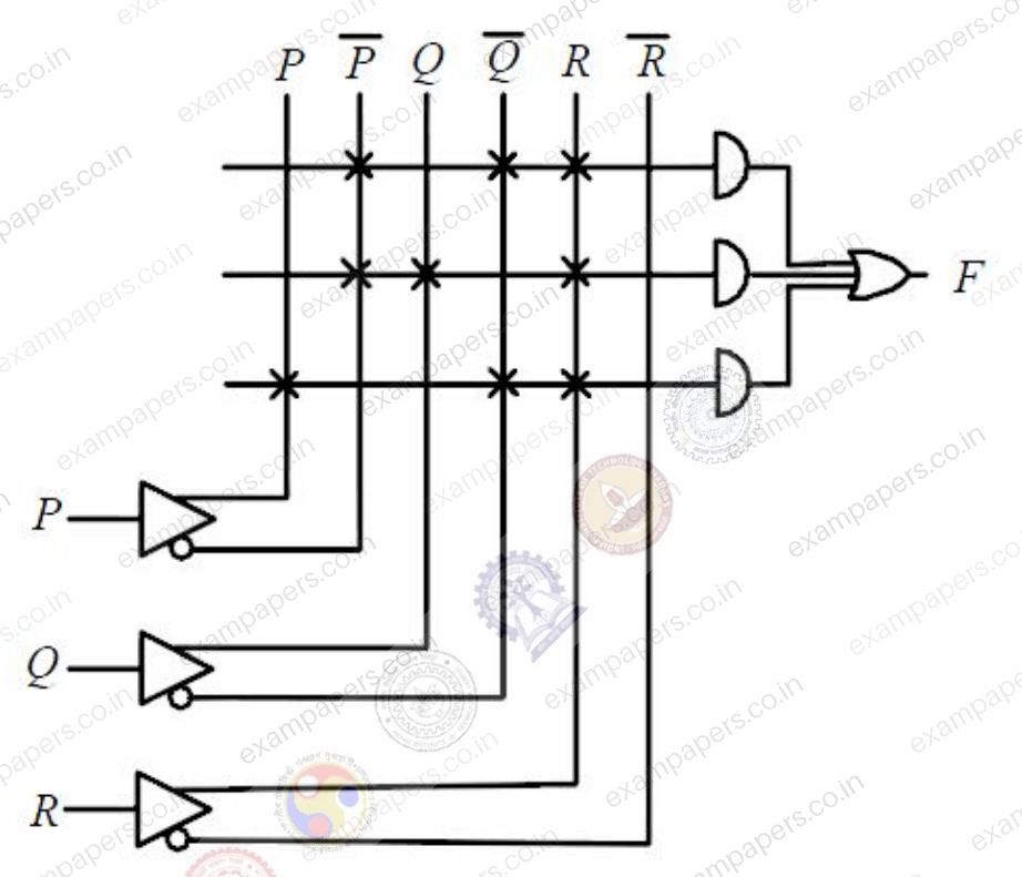
Your answerChoose one option.
Log in to check the answer
You can attempt this question now. Sign in to view the answer key, explanations and discussion.Log in to check answer