
Electronics and Communication Engineering
GATE ECE concept:mos-capacitor PYQs
Build your understanding with focused practice from past exam papers.
How to practice concept:mos-capacitor
Attempt a question, record the concept and assumptions, then check the available answer. Rework mistakes after revising the relevant concepts. Topic tags can overlap; review the question context.
Questions 1–5 of 5. Imported answers require independent review unless marked reviewed.
Question 61
Open questionECNAT2 marksNeeds review
Consider a MOS capacitor made with p-type silicon. It has an oxide thickness of 100 nm, a fixed positive oxide charge of
at the oxide-silicon interface, and a metal work function of 4.6 eV. Assume that the relative permittivity of the oxide is 4 and the absolute permittivity of free space is
. If the flatband voltage is 0 V, the work function of the p-type silicon (in eV, rounded off to two decimal places) is ______.Log in to check the answer
You can attempt this question now. Sign in to view the answer key, explanations and discussion.Log in to check answerQuestion 19
Open questionECMCQ1 markNeeds review
For a MOS capacitor,
and
are the flat-band voltage and the threshold voltage, respectively. The variation of the depletion width (
) for varying gate voltage (
) is best represented byYour answerChoose one option.
Log in to check the answer
You can attempt this question now. Sign in to view the answer key, explanations and discussion.Log in to check answerQuestion 34
Open questionECNAT1 markNeeds review
An ideal MOS capacitor (
-type semiconductor) is shown in the figure. The MOS capacitor is under strong inversion with
V. The corresponding inversion charge density (
) is 2.2
C/cm
. Assume oxide capacitance per unit area as
F/cm
. For
V, the value of
is _____
C/cm
(rounded off to one decimal place). 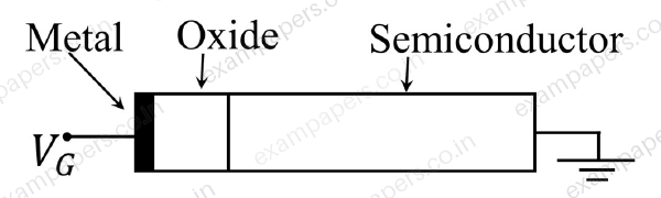
Log in to check the answer
You can attempt this question now. Sign in to view the answer key, explanations and discussion.Log in to check answerQuestion 32
Open questionECMCQ2 marksNeeds review
The band diagram of a
-type semiconductor with a band-gap of 1 eV is shown. Using this semiconductor, a MOS capacitor having
of
V,
of
nF/cm
and a metal work function of 3.87 eV is fabricated. There is no charge in the oxide. If the voltage across the capacitor is
, the magnitude of depletion charge per unit area (in C/cm
) is
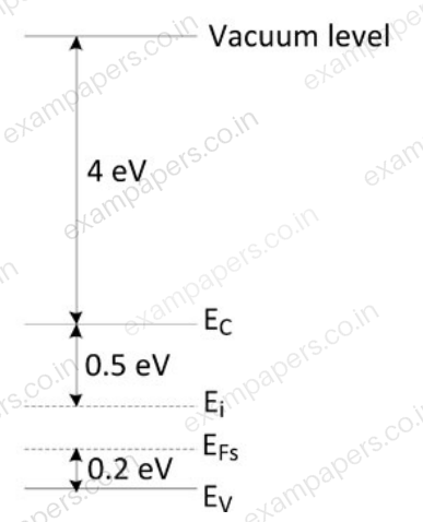
Your answerChoose one option.
Log in to check the answer
You can attempt this question now. Sign in to view the answer key, explanations and discussion.Log in to check answerQuestion 10
Open questionECMCQ1 markNeeds review
The figure shows the high-frequency C-V curve of a MOS capacitor (at T = 300 K) with
and no oxide charges. The flat-band, inversion, and accumulation conditions are represented, respectively, by the points
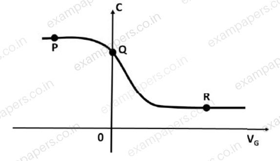
Your answerChoose one option.
Log in to check the answer
You can attempt this question now. Sign in to view the answer key, explanations and discussion.Log in to check answer