
Electronics and Communication Engineering
GATE ECE concept:flip-flops PYQs
Build your understanding with focused practice from past exam papers.
How to practice concept:flip-flops
Attempt a question, record the concept and assumptions, then check the available answer. Rework mistakes after revising the relevant concepts. Topic tags can overlap; review the question context.
Questions 1–9 of 9. Imported answers require independent review unless marked reviewed.
Question 27
Open questionECMSQ1 markNeeds review
A binary ripple counter is designed to count
to
. Which of the following is/are the number of flip-flops required to design the counter?Your answerSelect all correct options. You can choose more than one.
Log in to check the answer
You can attempt this question now. Sign in to view the answer key, explanations and discussion.Log in to check answerQuestion 35
Open questionECNAT1 markNeeds review
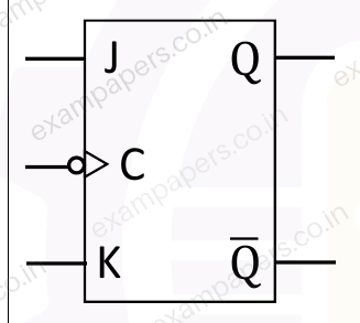
The negative edge triggered JK flip-flop in the Figure has J and K inputs tied to Logic High and a square wave of 10 cycles/second is applied to its clock (C) input. The frequency of the output Q (in cycles/second) is __. (rounded off to two decimal places)
Log in to check the answer
You can attempt this question now. Sign in to view the answer key, explanations and discussion.Log in to check answerQuestion 49
Open questionECMCQ2 marksNeeds review
A shift-left Shift Register (SR) and a D flip-flop are connected to a synchronized clock as shown in the Figure. Assume that the SR and D flip-flops are initially cleared and the XOR gate has no propagation delay.
Which of the following options gives the correct binary representation (
) of the content of the shift register immediately after the 5th clock transition (positive edge)? 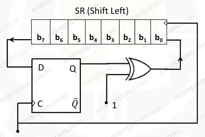
Your answerChoose one option.
Log in to check the answer
You can attempt this question now. Sign in to view the answer key, explanations and discussion.Log in to check answerQuestion 62
Open questionECNAT2 marksNeeds review
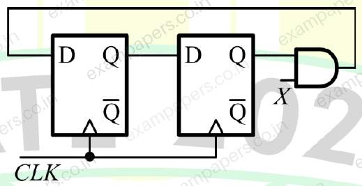
In the circuit shown below, the AND gate has a propagation delay of 1 ns. The edge-triggered flip-flops have a set-up time of 2 ns, a hold-time of 0 ns, and a clock-to-Q delay of 2 ns.
The maximum clock frequency (in MHz, rounded off to the nearest integer) such that there are no setup violations is __________.
Log in to check the answer
You can attempt this question now. Sign in to view the answer key, explanations and discussion.Log in to check answerQuestion 43
Open questionECMCQ2 marksNeeds review
For the circuit shown, the clock frequency is
and the duty cycle is 25%. For the signal at the Q output of the Flip-Flop, __________. 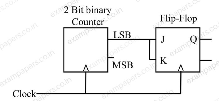
Your answerChoose one option.
Log in to check the answer
You can attempt this question now. Sign in to view the answer key, explanations and discussion.Log in to check answerQuestion 46
Open questionECNAT2 marksNeeds review
The propagation delay of the exclusive-OR (XOR) gate in the circuit in the figure is 3 ns. The propagation delay of all the flip-flops is assumed to be zero. The clock (Clk) frequency provided to the circuit is 500 MHz.
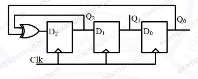
Starting from the initial value of the flip-flop outputs
with
, the minimum number of triggering clock edges after which the flip-flop outputs
becomes 100 (in integer) is ______.Log in to check the answer
You can attempt this question now. Sign in to view the answer key, explanations and discussion.Log in to check answerQuestion 19
Open questionECNAT1 markNeeds review
A traffic signal cycles from GREEN to YELLOW, YELLOW to RED and RED to GREEN. In each cycle, GREEN is turned on for 70 seconds, YELLOW is turned on for 5 seconds and the RED is turned on for 75 seconds. This traffic light has to be implemented using a finite state machine (FSM). The only input to this FSM is a clock of 5 second period. The minimum number of flip-flops required to implement this FSM is ______.
Log in to check the answer
You can attempt this question now. Sign in to view the answer key, explanations and discussion.Log in to check answerQuestion 46
Open questionECNAT2 marksNeeds review
In the circuit shown below, a positive edge-triggered D Flip-Flop is used for sampling input data
using clock
. The XOR gate outputs 3.3 volts for logic HIGH and 0 volts for logic LOW levels. The data bit and clock periods are equal and the value of
, where the parameters
and
are shown in the figure. Assume that the Flip-Flop and the XOR gate are ideal. 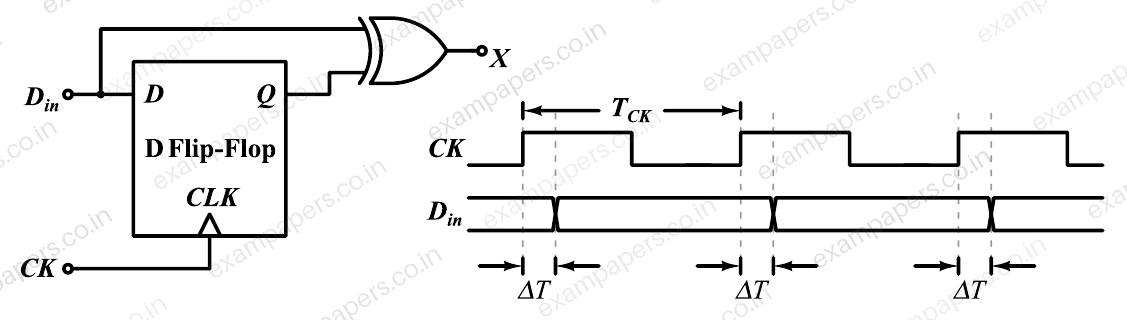
If the probability of input data bit (
) transition in each clock period is 0.3, the average value (in volts, accurate to two decimal places) of the voltage at node
, is ________.Log in to check the answer
You can attempt this question now. Sign in to view the answer key, explanations and discussion.Log in to check answerQuestion 46
Open questionECMCQ2 marksNeeds review
A finite state machine (FSM) is implemented using the D flip-flops A and B, and logic gates, as shown in the figure below. The four possible states of the FSM are
and
.
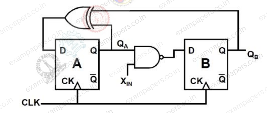
Assume that
is held at a constant logic level throughout the operation of the FSM. When the FSM is initialized to the state
and clocked, after a few clock cycles, it starts cycling throughYour answerChoose one option.
Log in to check the answer
You can attempt this question now. Sign in to view the answer key, explanations and discussion.Log in to check answer